
 My Inquiry
 My Account


STMicroelectronics LCP02-150B1RL
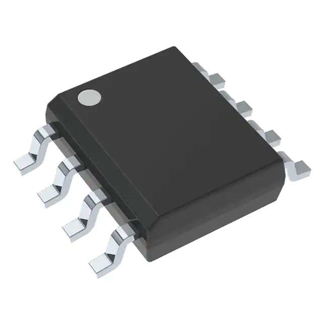
- Part No.:
- LCP02-150B1RL
- Manufacturer:
- STMicroelectronics
- Category:
- Thyristors
- Package:
- 8-SOIC (0.209", 5.30mm Width)
- Datasheet:
-
 LCP02-150B1RL.pdf
- Description:
- THYRISTOR 30A 8-SOIC
- Quantity:
- Payment:

- Shipping:

Inventory:3,627
Please send an inquiry. Send us your inquiry, and we will respond immediately.
Product details
Overview
LCP02-150B1RL from STMicroelectronics is a dual-thyristor crowbar protection IC designed for SLIC (Subscriber Line Interface Circuit) applications in telecom line cards. It provides programmable overvoltage protection on TIP and RING lines with independent negative (Gn) and positive (Gp) gate control, -110V to +95V firing range, 30A peak pulse current (10/1000µs), and UL497B approval (E136224) for ringing circuit protection.
For engineers reviewing the LCP02-150B1RL datasheet, LCP02-150B1RL pinout, LCP02-150B1RL application in SLIC protection, or LCP02-150B1RL equivalent for telecom surge suppression, this page delivers verified functional specifications, SO-8 Wide package details, gate-triggering behavior, thermal derating curves, and compliance mapping to ITU-T K20/K21, Bellcore GR-1089-CORE, FCC Part 68, and IEC61000-4-5 Level 4.
Technical Context
The LCP02-150B1RL implements two independent thyristor-based crowbar structures - one for negative surges (triggered via Gn at -110V to 0V), one for positive surges (triggered via Gp at 0V to +95V). Each path uses transistor-assisted gate triggering to reduce battery current during clamping.
It supports dual-battery SLIC topologies (±Vbat) and high-negative-voltage SLICs (-110V only), with dynamic switching voltage VDGL- ≤18V (negative) and VDGL+ ≤35V (positive) under 10/1000µs 30A surge, and maintains operation across -20°C to +85°C with junction-to-ambient thermal resistance of 150°C/W.
Key Specifications
| Parameter | Value and Actual Design Meaning |
|---|---|
| Peak pulse current | 30 A (10/1000µs); sustains full lightning surge energy without latch-up or degradation |
| Firing voltage range | -110 V to +95 V; enables protection across asymmetric dual-supply SLICs and high-negative-voltage systems |
| Gate trigger current | ≤5 mA (both Gn & Gp); ensures reliable turn-on with low-power bias networks |
| Holding current | ≥150 mA (IH⁻); guarantees automatic reset after surge decay below threshold |
| UL approval | UL497B (E136224); certifies suitability for primary telecom protection circuits per safety standard |
| Capacitance (LINE/GND) | 60 pF @ 1 MHz; minimizes signal distortion on voice/data lines while maintaining ESD robustness |
| Thermal resistance | 150 °C/W (Junction-to-Ambient); defines maximum power dissipation limit in SO-8 Wide package |
Pinout & Package
Package: SO-8 Wide (8-pin plastic surface-mount), 6.05 mm × 5.02 mm body, 1.27 mm pitch, 2.00 mm max height, UL94-V0 rated resin.
| Pin/Terminal | Circuit Role | Design Meaning |
|---|---|---|
| TIP | Line input (TIP side) | Connects to SLIC TIP terminal; subjected to bidirectional surge clamping via internal thyristors |
| RING | Line input (RING side) | Connects to SLIC RING terminal; shares same crowbar architecture as TIP with independent gate control |
| Gn | Negative gate control | Bias input for negative-thyristor trigger; connected to -Vbat to set -110V firing threshold |
| Gp | Positive gate control | Bias input for positive-thyristor trigger; connected to +Vbat to set +95V firing threshold |
| GND | Reference ground | Common return for gate bias, surge current sink, and thermal reference plane |
| NC | No connect | Pins 7 and 8 are internally unconnected; must remain floating or grounded per layout guidelines |
Key Features
| Feature | Design Value |
|---|---|
| Programmable dual-polarity thresholds | Independent Gn and Gp pins allow precise setting of -110V and +95V firing points for asymmetric SLIC supplies |
| Transistor-assisted gate drive | Reduces required gate current to ≤5 mA and lowers standby battery drain during normal operation |
| Temperature-stable holding current | IH⁻ ≥150 mA at 25°C with defined derating curve (Fig.2); prevents false turn-off during thermal transients |
| High-surge survivability | Rated for Bellcore GR-1089-CORE Second Level (5kV, 2/10µs, 500A) and IEC61000-4-5 Level 4 (10/1000µs, 100A) |
Applications
| Central Office (CO) Line Card Protection | ADSL G.Lite DSLAM Protection |
|---|---|
Use Scenario: Protecting analog front-end SLICs in carrier-grade central office line cards exposed to lightning-induced surges on copper loops. IC Role / Device Role / Timing Role: Crowbar protector that shorts TIP/RING to GND upon overvoltage detection, diverting >30A surge energy away from sensitive SLIC circuitry. Use Value: Enables compliance with Bellcore GR-1089-CORE Intrabuilding (800V, 2/10µs) and ITU-T K21 (4kV, 10/700µs) without external spark gaps or MOVs. | Use Scenario: Safeguarding ADSL G.Lite transceivers in residential DSLAMs where cost-sensitive, high-volume protection is required. IC Role / Device Role / Timing Role: Dual-thyristor protector with programmable thresholds, enabling single-device coverage of both positive and negative battery configurations. Use Value: Eliminates need for discrete TVS + SCR combinations, reducing BOM count by 2–3 components while maintaining UL497B certification. |
| Fiber-in-the-Loop (FITL) Remote Terminal | Wireless Local Loop (WLL) Base Station |
Use Scenario: Protecting hybrid fiber-copper interfaces in outdoor FITL remote terminals operating in harsh lightning-prone environments. IC Role / Device Role / Timing Role: High-reliability crowbar IC with 190V total differential voltage rating (∆Vbat), supporting ±95V/−110V SLIC designs. Use Value: Sustains 30A surge current at 10/1000µs without parameter shift, ensuring field longevity beyond 10-year telecom infrastructure deployments. | Use Scenario: Securing WLL base station line cards interfacing with legacy POTS wiring in rural deployments. IC Role / Device Role / Timing Role: Programmable protection IC allowing adaptation to varying local loop voltages (e.g., −105V to +85V) via external gate bias resistors. Use Value: Reduces qualification effort across regional variants-single LCP02-150B1RL design meets FCC Part 68 Type A (1500V) and Type B (1000V) requirements. |
Equivalent & Alternatives
The following parts are listed as comparable options for similar SLIC crowbar protection applications.
| Alternative Part | Technical Difference | Application Difference | Selection Advice |
|---|---|---|---|
| Protek Devices P0220SC | Single-direction (positive-only) thyristor; no Gn gate; 15A IPP (8/20µs); no UL497B listing | Limited to +Vbat-only SLICs; requires separate negative-path device for dual-supply systems | Select only when protecting unidirectional SLICs with fixed +48V supply and no negative rail |
| ON Semiconductor NUP4105 | Quad-channel TVS array; 12V clamping; 20A IPP (8/20µs); no crowbar latching or gate programming | Provides clamping only-not crowbar action-so SLIC remains powered during surge, risking latch-up | Use only for secondary-level transient suppression downstream of a primary crowbar like LCP02-150B1RL |
Compared with P0220SC and NUP4105, the LCP02-150B1RL uniquely delivers bidirectional, programmable, latching crowbar protection with certified UL497B compliance-enabling single-chip SLIC protection across global telecom standards without external biasing complexity or parallel device coordination.
Availability
LCP02-150B1RL is available at Aetrix Electronics and suitable for Central Office line cards, ADSL G.Lite DSLAMs, Fiber-in-the-Loop remote terminals, and Wireless Local Loop base stations requiring stable component supply with full traceability and long-term lifecycle support.
Supply support for LCP02-150B1RL includes scheduled delivery planning, volume procurement assistance, BOM continuity management, traceable sourcing, and lifecycle availability coordination for OEM customers, industrial embedded developers, connected-device designers, and electronics production programs.
Manufacturer
STMicroelectronics is a global semiconductor leader headquartered in Geneva, Switzerland, designing and manufacturing analog, power, microcontroller, and automotive ICs with vertical fabrication capability and ISO/TS 16949-certified operations.
The LCP02 series belongs to ST's Telecom Protection IC product line, engineered specifically for high-reliability, standards-compliant overvoltage protection in voice/data line interface circuits-including SLICs, CODECs, and hybrid couplers-where crowbar action, programmability, and regulatory certification are mandatory.
FAQ
What is the minimum recommended series resistor (Rs) between LCP02-150B1RL and SLIC to ensure safe operation under Bellcore GR-1089-CORE Second Level (5kV, 2/10µs)?
The LCP02-150B1RL itself does not specify a minimum Rs, but system-level testing per Bellcore requires limiting surge current to ≤500A. With a 5kV open-circuit surge and generator source impedance (Rg) of 2Ω, Rs ≥ 8Ω is required to keep Isurge ≤ 500A. Typical designs use 10–22Ω PTCs or fusible resistors placed adjacent to the IC to meet this requirement while surviving power contact tests.
Can LCP02-150B1RL be used in a single-supply (+48V only) SLIC configuration?
Yes-configure Gp to +48V and leave Gn open or tie to GND (per ST AN2127 guidance). The positive thyristor fires at ~+55V, providing robust protection. However, the negative path remains inactive, so external protection (e.g., TVS diode) is needed if negative transients exceed -5V. Full dual-supply advantage is lost, but functionality remains valid for +Vbat-only systems.
How does the 220nF capacitor (Cn/Cp) on Gn and Gp affect response time and clamping voltage?
The 220nF capacitors accelerate gate charging during fast-rising surges (e.g., 1.2/50µs), reducing dynamic breakover voltage at TIP/RING by up to 40% versus DC-triggered operation. They must be placed within 3mm of Gn/Gp pins and referenced directly to GND to minimize inductance. Values outside 100–470nF degrade timing margin or increase ringing.
Is LCP02-150B1RL compliant with RoHS and REACH regulations?
Yes-LCP02-150B1RL is manufactured in STMicroelectronics' RoHS-compliant facilities and meets EU Directive 2011/65/EU (RoHS 2) and Regulation (EC) No. 1907/2006 (REACH) with full substance declarations available in ST's official Product Change Notification (PCN) #18-0124 and material declaration report D180124.
LCP02-150B1RL Specifications
- Product attributes
- Attribute value
- Manufacturer:
- STMicroelectronics
- Package/Case:
- 8-SOIC (0.209", 5.30mm Width)
- Series:
- LCP
- Packaging:
- Tape & Reel (TR)
- Product Status:
- Active
- Voltage - Breakover:
- -
- Voltage - Off State:
- -
- Voltage - On State:
- -
- Current - Peak Pulse (8/20µs):
- -
- Current - Peak Pulse (10/1000µs):
- 30 A
- Current - Hold (Ih):
- 150 mA
- Number of Elements:
- 1
- Capacitance:
- -
- Grade:
- -
- Qualification:
- -
- Mounting Type:
- Surface Mount
- Supplier Device Package:
- 8-SO
LCP02-150B1RL FAQ
1.How can I place an order for LCP02-150B1RL through Aetrix?
Please submit a Request for Quotation (RFQ) for LCP02-150B1RL on Aetrix. Our sales agent will provide a competitive quotation and guide you through the order confirmation once you accept the terms.
2.Are the price and stock information for LCP02-150B1RL reliable?
The price and inventory of LCP02-150B1RL are updated periodically and may fluctuate due to market conditions. Stock and pricing data are typically refreshed every 24 hours. Quotation validity for LCP02-150B1RL is usually 5 days.
3.What payment methods are accepted for LCP02-150B1RL?
We accept Wire Transfer, PayPal, Credit Card, Western Union, MoneyGram, and Escrow for LCP02-150B1RL transactions.
Note: Certain payment methods may incur a processing fee.
4.How is shipping managed for LCP02-150B1RL?
LCP02-150B1RL orders can be shipped via leading logistics carriers, including DHL, UPS, FedEx, TNT, or Registered Mail.
Once your LCP02-150B1RL order is processed, you will receive an email with the shipment details and tracking number.
Note: Tracking information may take up to 24 hours to appear. Express delivery typically takes 3–5 business days.
5.How can I obtain technical support or documentation for LCP02-150B1RL?
For technical support, including LCP02-150B1RL datasheets, pinout diagrams, or application guidance, please contact our engineering support team. They can provide detailed documentation and assistance for your LCP02-150B1RL requirements.
6.How does Aetrix verify that LCP02-150B1RL is sourced from the original manufacturer or authorized distributors?
All LCP02-150B1RL products on Aetrix are procured from qualified distributors and authorized channels. Our dedicated quality assurance team conducts strict verification, including traceability checks and, if necessary, third-party testing. This ensures that LCP02-150B1RL meets industry standards.
7.What is the process for return or replacement of LCP02-150B1RL?
All LCP02-150B1RL units undergo pre-shipment inspection (PSI). If there is an issue with LCP02-150B1RL, returns or replacements are accepted under the following conditions:
1.Quantity discrepancies, incorrect items, or visible external defects (such as breakage or corrosion), acknowledged by Aetrix.
2.The issue is reported within 90 days of delivery.
3.The LCP02-150B1RL part is unused and in its original packaging.
Return procedure for LCP02-150B1RL:
1.Submit a request within 90 days.
2.Obtain a Return Material Authorization (RMA) from Aetrix.
LCP02-150B1RL Tags
-
TISP4015L1AJR-S
Bourns Inc.
-
TISP4015L1BJR-S
Bourns Inc.
-
SMP100LC-270
STMicroelectronics
-
TISP4240M3BJR-S
Bourns Inc.
-
SMP100LC-35
STMicroelectronics
-
SMP100LC-65
STMicroelectronics
-
SMP100LC-8
STMicroelectronics
-
TISP4P035L1NR-S
Bourns Inc.
-
TISP4350H3BJR-S
Bourns Inc.
-
TISP4011H1BJR-S
Bourns Inc.
-
SMP100LC-400
STMicroelectronics
-
P0300SALRP
Littelfuse Inc.
Tech Hub

A practical engineering guide to 3.3V and 5V logic compatibility, input thresholds, resistor dividers, translator ICs, MOSFET level shifting, I2C pull-ups, timing limits and power-sequencing risks.

The 74HC595 uses push-pull logic outputs, while the TPIC6B595 uses 50 V open-drain DMOS sinks for higher-power loads. This guide compares timing, current limits, 3.3 V interfacing, load wiring, thermal…

The 74HC595 converts serial data into eight stable parallel outputs. This guide covers pin functions, shift and storage timing, OE and MR behavior, drive-current limits, cascading, voltage compatibilit…

A technical comparison of level-sensitive latches and edge-triggered flip-flops, covering timing windows, setup and hold limits, master–slave operation, time borrowing, race-through, HDL inference and…

A D latch stores one bit while Enable controls when data can pass. This reference covers gate-level operation, truth tables, transparency, setup and hold timing, LE versus OE, common ICs and practical …

An SR latch stores one bit through cross-coupled feedback. This engineering reference covers NOR and NAND implementations, truth tables, forbidden-state recovery, gated operation, switch debouncing, fa…

Latch circuits retain one bit through feedback. This technical reference covers SR and D latches, truth tables, transparency, timing limits, latch-versus-flip-flop behavior, applications and common log…

An engineering guide to LED driver operation, constant-current and constant-voltage outputs, linear and switching topologies, dimming, IC selection, calculations, replacement compatibility, and fault c…

Operational amplifier guide covering op amp basics, feedback, ideal vs real op amps, common configurations, buffer circuits, offset, bias current, gain-bandwidth, slew rate, rail-to-rail limits and sel…

Jumper cables guide covering safe connection order, red and black clamp placement, final ground connection, cable gauge, length, clamp quality, copper vs CCA cables, jump starter comparison and battery…


