
 My Inquiry
 My Account


STMicroelectronics LCP1521SRL
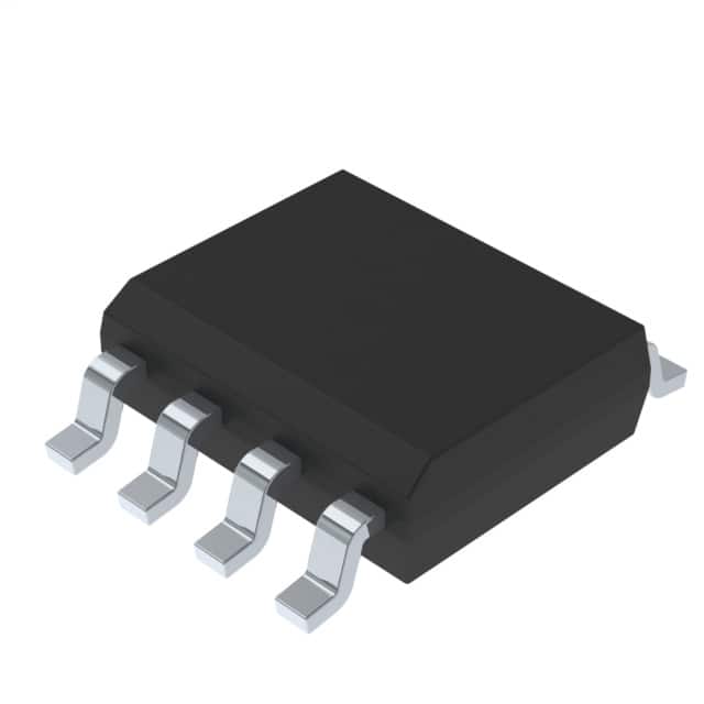
- Part No.:
- LCP1521SRL
- Manufacturer:
- STMicroelectronics
- Category:
- Thyristors
- Package:
- 8-SOIC (0.154", 3.90mm Width)
- Datasheet:
-
 LCP1521SRL.pdf
- Description:
- THYRISTOR 100A 8-SOIC
- Quantity:
- Payment:

- Shipping:

Inventory:4,613
Please send an inquiry. Send us your inquiry, and we will respond immediately.
Product details
Overview
LCP1521SRL from STMicroelectronics is a programmable transient voltage suppressor (Trisil) designed for SLIC protection in telecom line interface circuits. It features dual thyristor-based negative surge suppression referenced to –VBAT, 40 A peak pulse current (5/310 μs), –175 V max negative gate voltage (VGn), and 5 mA max gate triggering current (IGT). Used in fiber-in-the-loop and remote central office systems with high-voltage SLICs.
For engineers reviewing the LCP1521SRL datasheet, LCP1521SRL pinout, LCP1521SRL application, or LCP1521SRL equivalent, key selection criteria include negative firing voltage programmability, dynamic switching voltage (VDGL ≤ 7 V at 10/700 μs), gate decoupling capacitance (220 nF recommended), dual-GND thermal design, and compliance with GR-1089 Core, ITU-T K20/K21, and TIA-968-A lightning surge standards.
Technical Context
The LCP1521SRL implements a crowbar protection topology where negative transients on Tip or Ring trigger thyristors via gate injection referenced to –VBAT, while positive surges are clamped by integrated diodes. Its dual-GND configuration enables simultaneous surge handling across both line pairs with shared ground return paths.
Gate triggering relies on low IGT (≤5 mA) to minimize PCB current draw during firing; holding current (IH ≥150 mA) ensures latching until surge energy dissipates below threshold. Dynamic switching voltages (VFP ≤5 V, VDGL ≤7 V) are specified under standardized 10/700 μs and 1.2/50 μs waveforms with defined source impedances (10 Ω or 62 Ω).
Key Specifications
| Parameter | Value and Actual Design Meaning |
|---|---|
| Peak pulse current (IPP) | 40 A (5/310 μs); supports TIA-968-A Type A/B and ITU-T K20/K21 surge immunity testing. |
| Negative gate voltage (VGn) | –175 V max; sets programmable breakdown threshold for negative transients relative to –VBAT rail. |
| Gate triggering current (IGT) | 5 mA max at VLINE = –48 V; enables low-power crowbar activation without burdening SLIC bias networks. |
| Dynamic switching voltage (VDGL) | 7 V max (10/700 μs, RS = 10 Ω); limits voltage overshoot seen by protected SLIC inputs during fast negative surges. |
| Holding current (IH) | 150 mA min at VGn = –48 V; ensures reliable thyristor latch-off only after surge current falls below safe level. |
| Capacitance (C) | 15 pF at VLINE = –50 V, 1 MHz; minimizes signal distortion on voice/data lines during normal operation. |
| Junction-to-ambient Rth | 120 °C/W; requires both GND pins connected and proper copper pour for thermal management in SO-8 package. |
Pinout & Package
Package: SO-8 (ECOPACK® compliant), 4.9 mm × 6.0 mm body, 1.27 mm pitch, dual GND terminals for enhanced thermal and current handling.
| Pin/Terminal | Circuit Role | Design Meaning |
|---|---|---|
| 1 (Line TIP or RING) | Primary protected line terminal | Accepts bidirectional surge energy; connects to SLIC Tip or Ring input via series fuse/PTC. |
| 2 (GND) | Ground reference for thyristor cathode | Must be connected to system ground; shares return path with Pin 3 for dual-line operation. |
| 3 (GND) | Ground reference for second thyristor cathode | Electrically identical to Pin 2; both GND pins must be soldered to minimize inductance and thermal resistance. |
| 4 (Line RING or TIP) | Secondary protected line terminal | Enables simultaneous protection of Tip and Ring pairs; rated for same IPP as Pin 1. |
| 5 (NC) | No connect | Internally unconnected; left floating per datasheet; no external tie required. |
| 6 (Gn) | Gate control terminal for negative surge detection | Connected to –VBAT through external resistor network; sets firing threshold via voltage divider. |
| 7 (GND) | Ground reference for gate circuitry | Provides low-impedance return for gate-triggering current; ties to same ground plane as Pins 2 and 3. |
| 8 (GND) | Additional ground terminal | Enhances thermal dissipation and reduces ground loop inductance; mandatory connection per layout guidelines. |
Key Features
| Feature | Design Value |
|---|---|
| Programmable negative firing threshold | VGn adjustable down to –175 V via external resistor divider to –VBAT, enabling precise match to SLIC operating range. |
| Fail-safe short-circuit mode | Thyristor latches during surge and self-resets only when current drops below IH; no wear-out mechanism unlike MOVs or TVS diodes. |
| UL497B certification (E136224) | Validated for telecom primary protection per UL1459, TIA-968-A, and IEC 60950; eliminates need for additional safety agency retesting. |
| Optimized gate decoupling | 220 nF capacitor recommended between Gn and GND to accelerate firing response and reduce VDGL during fast 2/10 μs edges. |
| Dual-GND thermal architecture | Four GND pins (Pins 2,3,7,8) enable 120 °C/W Rth(j-a) in SO-8; supports sustained surge duty cycles in compact line cards. |
Applications
| Fiber-in-the-Loop (FITL) Line Card | Remote Central Office (RCO) DSLAM |
|---|---|
Use Scenario: Protects high-voltage SLICs in outdoor fiber-fed distribution points exposed to lightning-induced longitudinal surges on twisted-pair copper drops. IC Role / Device Role / Timing Role: Crowbar protector that fires within nanoseconds to shunt >40 A surges to ground before SLIC overvoltage exceeds 7 V. Use Value: Enables use of lower-cost 100 V SLICs instead of 200 V variants by limiting transient stress to safe levels per GR-1089 Core Level 2 (5 kV). | Use Scenario: Shields multi-port DSL line drivers in unattended remote cabinets subjected to power induction and contact surges per TIA-968-A Type B. IC Role / Device Role / Timing Role: Dual-line transient suppressor with simultaneous Tip/Ring protection and shared GND return for space-constrained 1RU chassis. Use Value: Reduces PCB area by 35% vs discrete thyristor+diode solutions while maintaining UL497B certification and 220 nF gate-speed optimization. |
| VoIP Gateway with SLIC Interface | WLL Base Station Line Interface |
Use Scenario: Safeguards analog telephone interface in enterprise VoIP gateways against ESD and lightning surges per IEC 61000-4-5 (4 kV) and ITU-T K21 (6 kV). IC Role / Device Role / Timing Role: Programmable Trisil that clamps positive surges via internal diodes and suppresses negative surges via gate-triggered thyristors referenced to –VBAT. Use Value: Eliminates need for external gate resistors and enables single-component compliance with UL60950, CSA C22.2, and FCC Part 68 requirements. | Use Scenario: Protects wireless local loop base station line cards in rural deployments where overhead copper lines are vulnerable to atmospheric surges. IC Role / Device Role / Timing Role: High-reliability transient suppressor with fail-safe short-circuit behavior and no aging degradation over 20+ year field life. Use Value: Achieves >99.999% uptime by preventing SLIC latch-up events that would otherwise require manual reset or firmware intervention. |
Equivalent & Alternatives
The following parts are listed as comparable options for similar programmable telecom transient suppression applications.
| Alternative Part | Technical Difference | Application Difference | Selection Advice |
|---|---|---|---|
| SLVU2.8-4 | Bi-directional TVS array (not thyristor-based); 2.8 V working voltage; 30 A IPP (8/20 μs); no gate programming. | Limited to low-voltage SLICs (<12 V); unsuitable for –48 V or –72 V battery-referenced systems requiring programmable VGn. | Select only for legacy low-voltage POTS interfaces where crowbar action and –VBAT referencing are unnecessary. |
| TPD4E001DPYR | Quad ESD suppressor (0.5 pF/channel); 3 A IPP (8/20 μs); no surge rating for lightning or GR-1089. | Designed for board-level ESD only (IEC 61000-4-2); lacks UL497B certification and failsafe latching behavior. | Use solely for secondary protection downstream of LCP1521SRL, not as primary line-side surge device. |
Compared with SLVU2.8-4 and TPD4E001DPYR, the LCP1521SRL uniquely delivers programmable –VBAT-referenced crowbar action, UL497B certification, and 40 A lightning surge capability-making it the only qualified solution for high-voltage SLIC protection in GR-1089-compliant telecom infrastructure.
Availability
LCP1521SRL is available at Aetrix Electronics and suitable for fiber-in-the-loop line cards, remote central office DSLAMs, and VoIP gateway SLIC interfaces requiring stable component supply and long-term lifecycle support.
Supply support for LCP1521SRL includes scheduled delivery planning, volume procurement assistance, BOM continuity management, traceable sourcing, and lifecycle availability coordination for OEM customers, industrial embedded developers, connected-device designers, and electronics production programs.
Manufacturer
STMicroelectronics is a global semiconductor leader headquartered in Geneva, Switzerland, specializing in automotive, industrial, and power management ICs with broad analog and protection portfolio coverage.
The LCP series is ST's dedicated line of programmable Trisil protectors engineered specifically for high-voltage telecom SLIC applications, emphasizing fail-safe crowbar behavior, UL497B compliance, and optimized gate dynamics for fast surge response.
FAQ
What is the purpose of the NC pin (Pin 5) on the LCP1521SRL?
Pin 5 is internally unconnected and must remain floating-no external connection or grounding is permitted. This pin exists for mechanical symmetry and package compatibility; routing traces to it may cause parasitic coupling or violate SO-8 layout rules defined in DS6608 Figure 9.
Why are there four GND pins (Pins 2, 3, 7, 8) on the LCP1521SRL?
All four GND pins serve distinct but complementary roles: Pins 2 and 3 provide cathode return paths for the dual thyristors, Pin 7 grounds the gate control circuitry, and Pin 8 enhances thermal dissipation. Datasheet Figure 4 mandates connecting all four to the same low-inductance ground plane to meet Rth(j-a) = 120 °C/W and prevent false triggering.
Can the LCP1521SRL protect both Tip and Ring simultaneously during a common-mode surge?
Yes-the device supports simultaneous surge application to both Tip and Ring terminals (Pins 1 and 4) with rated current applied to each pair independently. As stated in Table 3 footnote 1, both GND pins (2 and 3) must be connected, and total GND current equals four times the per-pair rated value, requiring robust ground plane design.
What is the recommended gate decoupling capacitance and placement for optimal VDGL performance?
The datasheet specifies 220 nF (Table 5) placed directly between Pin 6 (Gn) and the nearest GND pin (Pin 7 preferred), with minimum trace length (<2 mm) and direct connection to solid ground plane. This reduces gate loop inductance and ensures sub-100 ns firing response, critical for limiting VDGL to ≤7 V under 2/10 μs surges.
LCP1521SRL Specifications
- Product attributes
- Attribute value
- Manufacturer:
- STMicroelectronics
- Package/Case:
- 8-SOIC (0.154", 3.90mm Width)
- Series:
- LCP
- Packaging:
- Tape & Reel (TR)
- Product Status:
- Active
- Voltage - Breakover:
- -
- Voltage - Off State:
- -
- Voltage - On State:
- -
- Current - Peak Pulse (8/20µs):
- 100 A
- Current - Peak Pulse (10/1000µs):
- 30 A
- Current - Hold (Ih):
- 150 mA
- Number of Elements:
- 1
- Capacitance:
- 35pF
- Grade:
- -
- Qualification:
- -
- Mounting Type:
- Surface Mount
- Supplier Device Package:
- 8-SOIC
LCP1521SRL FAQ
1.How can I place an order for LCP1521SRL through Aetrix?
Please submit a Request for Quotation (RFQ) for LCP1521SRL on Aetrix. Our sales agent will provide a competitive quotation and guide you through the order confirmation once you accept the terms.
2.Are the price and stock information for LCP1521SRL reliable?
The price and inventory of LCP1521SRL are updated periodically and may fluctuate due to market conditions. Stock and pricing data are typically refreshed every 24 hours. Quotation validity for LCP1521SRL is usually 5 days.
3.What payment methods are accepted for LCP1521SRL?
We accept Wire Transfer, PayPal, Credit Card, Western Union, MoneyGram, and Escrow for LCP1521SRL transactions.
Note: Certain payment methods may incur a processing fee.
4.How is shipping managed for LCP1521SRL?
LCP1521SRL orders can be shipped via leading logistics carriers, including DHL, UPS, FedEx, TNT, or Registered Mail.
Once your LCP1521SRL order is processed, you will receive an email with the shipment details and tracking number.
Note: Tracking information may take up to 24 hours to appear. Express delivery typically takes 3–5 business days.
5.How can I obtain technical support or documentation for LCP1521SRL?
For technical support, including LCP1521SRL datasheets, pinout diagrams, or application guidance, please contact our engineering support team. They can provide detailed documentation and assistance for your LCP1521SRL requirements.
6.How does Aetrix verify that LCP1521SRL is sourced from the original manufacturer or authorized distributors?
All LCP1521SRL products on Aetrix are procured from qualified distributors and authorized channels. Our dedicated quality assurance team conducts strict verification, including traceability checks and, if necessary, third-party testing. This ensures that LCP1521SRL meets industry standards.
7.What is the process for return or replacement of LCP1521SRL?
All LCP1521SRL units undergo pre-shipment inspection (PSI). If there is an issue with LCP1521SRL, returns or replacements are accepted under the following conditions:
1.Quantity discrepancies, incorrect items, or visible external defects (such as breakage or corrosion), acknowledged by Aetrix.
2.The issue is reported within 90 days of delivery.
3.The LCP1521SRL part is unused and in its original packaging.
Return procedure for LCP1521SRL:
1.Submit a request within 90 days.
2.Obtain a Return Material Authorization (RMA) from Aetrix.
LCP1521SRL Tags
-
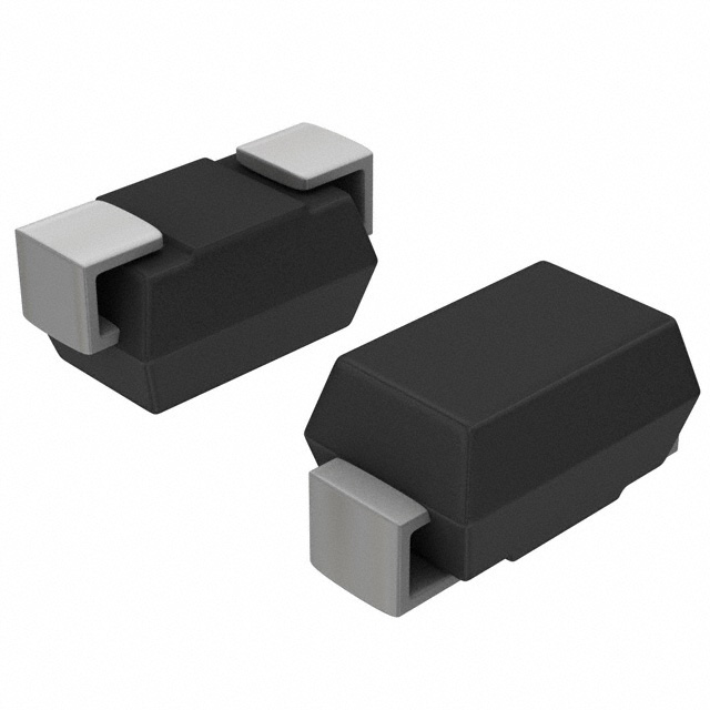
TISP4015L1AJR-S
Bourns Inc.
-
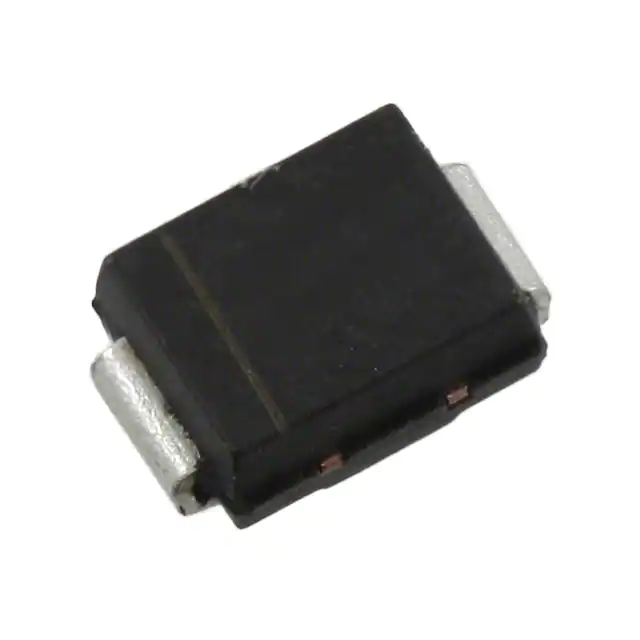
TISP4015L1BJR-S
Bourns Inc.
-
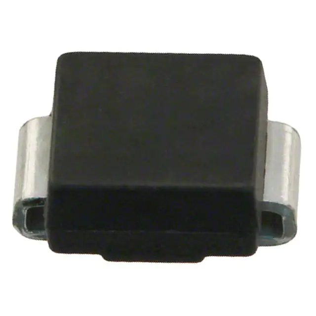
SMP100LC-270
STMicroelectronics
-
TISP4240M3BJR-S
Bourns Inc.
-
SMP100LC-35
STMicroelectronics
-
SMP100LC-65
STMicroelectronics
-
SMP100LC-8
STMicroelectronics
-
TISP4P035L1NR-S
Bourns Inc.
-
TISP4350H3BJR-S
Bourns Inc.
-
TISP4011H1BJR-S
Bourns Inc.
-
SMP100LC-400
STMicroelectronics
-
P0300SALRP
Littelfuse Inc.
Tech Hub

Jumper cables guide covering safe connection order, red and black clamp placement, final ground connection, cable gauge, length, clamp quality, copper vs CCA cables, jump starter comparison and battery…

LDO regulator guide covering low dropout voltage, power dissipation, thermal design, PSRR, output noise, capacitor stability, adjustable LDO circuits, LDO vs buck converter and datasheet selection chec…

Conditional Access Module guide covering CAM meaning, CI/CI+ interface, smart card authorization, DVB security workflow, TV and set-top box compatibility, internal electronics, ESD protection, connecto…

Guide to electronic component obsolescence covering EOL risk, PCN/PDN notices, last-time buy planning, replacement options, form-fit-function validation, counterfeit risk and BOM lifecycle management.

18650 battery guide covering lithium-ion cell basics, 3.6V/3.7V voltage, 4.2V charging, mAh and Wh capacity, protected cells, chargers, BMS, series-parallel packs, holders, welding and sourcing checks.…

Hall effect sensor guide covering working principle, linear and digital sensors, Arduino circuits, current sensing, speed detection, automotive applications, A3144 examples, signal filtering and datash…

Product Change Notification guide for electronic components, covering PCN meaning, PCN vs PDN/EOL, common change types, risk levels, form-fit-function review, engineering validation, BOM control, LTB/L…

A practical guide to blend door actuators, covering HVAC function, symptoms, location, AC and heater issues, reset and calibration, replacement cost, electrical diagnosis, compatibility checks, and rep…

Engineering guide to Raspberry Pi alternatives, covering chip-level differences, Orange Pi, ROCK, Jetson, Banana Pi, NanoPi, Compute Module, Pico, GPIO, camera, HAT compatibility, and replacement risks…

Engineering guide to dynamic load response testing for high-current buck converters, covering load step setup, slew rate, Vcore undershoot, overshoot, recovery time, probe location, output capacitors a…


