
 My Inquiry
 My Account


Texas Instruments LMH2110TMX/NOPB
- Part No.:
- LMH2110TMX/NOPB
- Manufacturer:
- Texas Instruments
- Category:
- RF Detectors
- Package:
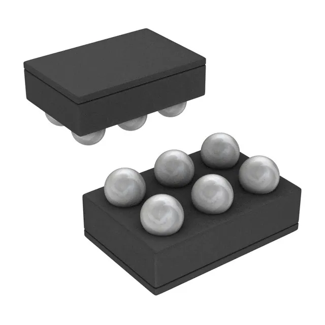
- 6-WFBGA, DSBGA
- Datasheet:
-
 LMH2110TMX/NOPB.pdf
- Description:
- IC RF DETECT 50MHZ-8GHZ 6DSBGA
- Quantity:
- Payment:

- Shipping:

Inventory:5,925
Please send an inquiry. Send us your inquiry, and we will respond immediately.
Product details
Overview
LMH2110TMX/NOPB from Texas Instruments is an 8-GHz logarithmic RMS power detector optimized for accurate RF power measurement of high-PAR modulated signals (e.g., W-CDMA, LTE) in cellular front-end modules. It delivers ±0.5 dB log conformance over 45 dB dynamic range (–40 dBm to +5 dBm), operates from 2.7 V to 5 V, and features shutdown control via EN pin with high-impedance output during sleep.
For engineers reviewing the LMH2110TMX/NOPB datasheet, LMH2110TMX/NOPB pinout, LMH2110TMX/NOPB application, or LMH2110TMX/NOPB equivalent, key selection criteria include its RMS-based modulation independence, temperature-insensitive slope (±0.25 dB), 6-bump DSBGA package footprint, and compatibility with directional couplers or resistive dividers in multi-band RF power control loops.
Technical Context
The LMH2110TMX/NOPB implements a true RMS detection architecture using internal exponential conversion and precision analog processing, ensuring modulation-independent response across W-CDMA, LTE, and OFDMA waveforms. Its integrated LDO decouples output accuracy from supply ripple, enabling stable operation under noisy DC conditions.
It supports RF input frequencies from 50 MHz to 8 GHz with frequency-dependent log slope (41.8–47.1 mV/dB) and intercept (–38.6 to –19.9 dBm), calibrated per band. The EN-controlled shutdown reduces supply current to <6.1 µA while placing OUT in high-impedance state to preserve external filter charge.
Key Specifications
| Parameter | Value and Actual Design Meaning |
|---|---|
| RF Frequency Range | 50 MHz to 8 GHz - enables single-detector coverage across GSM/EDGE, CDMA, W-CDMA, LTE, and 5G sub-6 GHz bands. |
| Dynamic Range | 45 dB (–40 dBm to +5 dBm) - supports full transmit power monitoring from low-level pilot signals to peak PA output. |
| Log Conformance Error | ±0.5 dB max - ensures direct dBm-to-voltage translation without per-unit calibration in production. |
| Temperature Drift | ±0.25 dB over –40°C to +85°C - eliminates need for thermal compensation circuitry in baseband power control loops. |
| Supply Voltage Range | 2.7 V to 5 V - compatible with both 3.3 V and 5 V system rails, including battery-backed RF sections. |
| Shutdown Current | <6.1 µA at VDD = 4.5 V - minimizes standby power in always-on RF monitoring paths. |
| Turnon Time | 19 µs max - supports fast AGC loop response and burst-mode transmission timing. |
Pinout & Package
LMH2110TMX/NOPB uses a 6-bump DSBGA (YFQ) package measuring 1.27 mm × 0.87 mm with 0.4 mm bump pitch. The ultra-compact footprint supports high-density RF layout adjacent to power amplifiers and couplers.
| Pin/Terminal | Circuit Role | Design Meaning |
|---|---|---|
| A1 | VDD | Positive supply input - connects to regulated 2.7–5 V rail; internally powers LDO and core detector. |
| A2 | OUT | Analog output voltage - ground-referenced linear-in-dB voltage (3 mV to 1.96 V) proportional to RF input power. |
| B1 | RFIN | RF input terminal - 50 Ω internally terminated; accepts CW or modulated signals from 50 MHz to 8 GHz. |
| B2, C1 | GND | Power ground - dual ground bumps reduce impedance and improve RF return path integrity. |
| C2 | EN | Logic enable input - HIGH (>1.1 V) activates detector; LOW (<0.6 V) enables shutdown with high-Z OUT. |
Key Features
| Feature | Design Value |
|---|---|
| Logarithmic RMS Response | True RMS detection topology ensures accurate power measurement regardless of signal crest factor or modulation format (W-CDMA, LTE, QAM). |
| Multi-Band Operation | Validated performance from 50 MHz to 8 GHz - eliminates need for band-switched detectors in multi-mode transceivers. |
| Integrated LDO | On-chip low-dropout regulator rejects supply noise up to 56 dB, enabling direct connection to noisy digital or PA supply rails. |
| Shutdown Mode | EN-controlled sleep mode reduces current to <6.1 µA and disables OUT driver - preserves external RC filter charge and saves system power. |
| High Temp Stability | ±0.25 dB total error over –40°C to +85°C - enables uncalibrated operation in outdoor small cells and automotive telematics. |
Applications
| Cellular Transmitter Power Control | Base Station RF Monitoring |
|---|---|
|
Use Scenario: Real-time closed-loop control of PA output power in LTE/W-CDMA handset front-end modules using directional coupler feedback. IC Role / Device Role / Timing Role: RMS power detector providing dBm-linear voltage to baseband processor's ADC for AGC computation. Use Value: Enables modulation-independent power setting across 64-QAM, 16-QAM, and QPSK LTE waveforms without recalibration. |
Use Scenario: Continuous RF output power verification in macrocell and microcell BTS transmitters operating across 700 MHz–3.8 GHz bands. IC Role / Device Role / Timing Role: High-speed power monitor feeding back to FPGA-based safety interlock logic for PA protection. Use Value: 19 µs turnon time supports rapid fault detection during PA ramp-up; ±0.5 dB accuracy meets 3GPP TR 37.842 monitoring tolerance. |
| Wi-Fi 6/6E Front-End Calibration | Test & Measurement Signal Leveling |
|
Use Scenario: Production-line RF power calibration of Wi-Fi 6E (5.925–7.125 GHz) front-end ICs using integrated coupler sampling. IC Role / Device Role / Timing Role: Reference-grade RMS detector interfaced to automated test equipment (ATE) for swept-power characterization. Use Value: 45 dB dynamic range covers full Wi-Fi transmit range (–30 dBm to +20 dBm); 8 GHz bandwidth validates EIRP compliance. |
Use Scenario: Stabilizing output level of RF signal generators and vector network analyzers during swept-frequency measurements. IC Role / Device Role / Timing Role: Feedback sensor in automatic level control (ALC) loop driving variable attenuator or VGA gain stage. Use Value: Modulation-independent response ensures consistent leveling for OFDM, pulsed radar, and CW signals without waveform-specific tuning. |
Equivalent & Alternatives
The following parts are listed as comparable options for similar logarithmic RMS power detection applications.
| Alternative Part | Technical Difference | Application Difference | Selection Advice |
|---|---|---|---|
| ADL5511ACPZ-R7 | Wider bandwidth (up to 10 GHz), higher supply current (12 mA active), no integrated LDO - requires clean 3.3 V supply. | Better suited for millimeter-wave test equipment; less tolerant of noisy PA supply rails than LMH2110TMX/NOPB. | Select when >8 GHz coverage or superior high-frequency log conformance is required; verify external supply filtering. |
| MAX2016ETE+ | Narrower RF range (40 MHz–2.5 GHz), lower dynamic range (35 dB), integrated temperature compensation - optimized for 2G/3G infrastructure. | Limited to sub-3 GHz bands; not suitable for LTE-A carrier aggregation or 5G NR FR1 deployments. | Choose for cost-sensitive legacy infrastructure where 8 GHz capability is unnecessary and temperature drift must be actively corrected. |
Compared with ADL5511ACPZ-R7 and MAX2016ETE+, the LMH2110TMX/NOPB uniquely balances 8 GHz bandwidth, 45 dB dynamic range, integrated LDO, and ultra-low shutdown current in a 1.27 mm × 0.87 mm DSBGA - making it optimal for space-constrained, multi-band mobile and small-cell RF power control where supply noise and thermal stability are critical.
Availability
LMH2110TMX/NOPB is available at Aetrix Electronics and suitable for cellular handset design, base station RF subsystems, and Wi-Fi 6E front-end calibration requiring stable component supply, long-term lifecycle support, and traceable sourcing.
Supply support for LMH2110TMX/NOPB includes scheduled delivery planning, volume procurement assistance, BOM continuity management, traceable sourcing, and lifecycle availability coordination for OEM customers, industrial embedded developers, connected-device designers, and electronics production programs.
Manufacturer
Texas Instruments is a global semiconductor leader specializing in analog, embedded processing, and connectivity technologies, with decades of RF IC innovation and broad manufacturing scale.
The LMH2110TMX/NOPB belongs to TI's high-frequency RF detector product line, designed specifically for accurate, modulation-agnostic power measurement in multi-standard wireless transmitters and infrastructure equipment.
FAQ
What is the RF input impedance of the LMH2110TMX/NOPB, and is external matching required?
The LMH2110TMX/NOPB features a 50 Ω internally terminated RF input (RFIN) across its full 50 MHz–8 GHz range, as confirmed by impedance plots in the datasheet. No external matching network is needed - the device is designed for direct connection to 50 Ω source impedances such as directional couplers or resistive dividers. This simplifies PCB layout and eliminates tuning complexity in production.
Does the LMH2110TMX/NOPB require calibration for different modulation formats like LTE 64-QAM or W-CDMA Release 8?
No, the LMH2110TMX/NOPB does not require per-modulation calibration. Its true RMS detection architecture provides modulation-independent response, with input-referred variation of only 0.08 dB for W-CDMA and 0.19 dB for LTE under specified power ranges. This enables single-point calibration across all supported waveforms, reducing factory test time and firmware overhead.
How does the LMH2110TMX/NOPB behave during shutdown, and what happens to the OUT pin?
When EN is driven LOW (<0.6 V), the LMH2110TMX/NOPB enters shutdown mode, drawing <6.1 µA supply current. Critically, the OUT pin transitions to high-impedance state - it neither sources nor sinks current - preserving charge on any external RC filter capacitor. This prevents discharge-induced voltage droop and allows fast wake-up without recharging delays.
What is the typical output voltage range of the LMH2110TMX/NOPB, and how does it map to RF input power?
The LMH2110TMX/NOPB outputs a ground-referenced voltage linearly proportional to RF input power in dBm. At RFIN = –40 dBm (50 MHz), VOUT ≈ 3 mV; at RFIN = +5 dBm (50 MHz), VOUT ≈ 1.96 V. The slope is typically 44.3 mV/dB with intercept –38.3 dBm, enabling direct dBm calculation: PdBm = (VOUT – VINT) / KSLOPE.
Can the LMH2110TMX/NOPB operate from a 3.3 V supply, and how does supply voltage affect accuracy?
Yes, the LMH2110TMX/NOPB operates fully across 2.7 V to 5 V. Its integrated LDO ensures supply rejection ratio (PSRR) of 56 dB, meaning output voltage accuracy remains unaffected by supply ripple or droop. Measured log conformance error and slope variation are specified worst-case across the entire supply range - no derating or recalibration is needed when using 3.3 V.
LMH2110TMX/NOPB Specifications
- Product attributes
- Attribute value
- Manufacturer:
- Texas Instruments
- Series:
- -
- Packaging:
- Tape & Reel (TR)
- Product Status:
- Active
- Frequency:
- 50MHz ~ 8GHz
- RF Type:
- GSM, EDGE, CDMA
- Input Range:
- -40dBm ~ 5dBm
- Accuracy:
- ±0.5dB
- Voltage - Supply:
- 2.7V ~ 5V
- Mounting Type:
- -
- Supplier Device Package:
- Surface Mount
- Current - Supply:
- 6-DSBGA
LMH2110TMX/NOPB FAQ
1.How can I place an order for LMH2110TMX/NOPB through Aetrix?
Please submit a Request for Quotation (RFQ) for LMH2110TMX/NOPB on Aetrix. Our sales agent will provide a competitive quotation and guide you through the order confirmation once you accept the terms.
2.Are the price and stock information for LMH2110TMX/NOPB reliable?
The price and inventory of LMH2110TMX/NOPB are updated periodically and may fluctuate due to market conditions. Stock and pricing data are typically refreshed every 24 hours. Quotation validity for LMH2110TMX/NOPB is usually 5 days.
3.What payment methods are accepted for LMH2110TMX/NOPB?
We accept Wire Transfer, PayPal, Credit Card, Western Union, MoneyGram, and Escrow for LMH2110TMX/NOPB transactions.
Note: Certain payment methods may incur a processing fee.
4.How is shipping managed for LMH2110TMX/NOPB?
LMH2110TMX/NOPB orders can be shipped via leading logistics carriers, including DHL, UPS, FedEx, TNT, or Registered Mail.
Once your LMH2110TMX/NOPB order is processed, you will receive an email with the shipment details and tracking number.
Note: Tracking information may take up to 24 hours to appear. Express delivery typically takes 3–5 business days.
5.How can I obtain technical support or documentation for LMH2110TMX/NOPB?
For technical support, including LMH2110TMX/NOPB datasheets, pinout diagrams, or application guidance, please contact our engineering support team. They can provide detailed documentation and assistance for your LMH2110TMX/NOPB requirements.
6.How does Aetrix verify that LMH2110TMX/NOPB is sourced from the original manufacturer or authorized distributors?
All LMH2110TMX/NOPB products on Aetrix are procured from qualified distributors and authorized channels. Our dedicated quality assurance team conducts strict verification, including traceability checks and, if necessary, third-party testing. This ensures that LMH2110TMX/NOPB meets industry standards.
7.What is the process for return or replacement of LMH2110TMX/NOPB?
All LMH2110TMX/NOPB units undergo pre-shipment inspection (PSI). If there is an issue with LMH2110TMX/NOPB, returns or replacements are accepted under the following conditions:
1.Quantity discrepancies, incorrect items, or visible external defects (such as breakage or corrosion), acknowledged by Aetrix.
2.The issue is reported within 90 days of delivery.
3.The LMH2110TMX/NOPB part is unused and in its original packaging.
Return procedure for LMH2110TMX/NOPB:
1.Submit a request within 90 days.
2.Obtain a Return Material Authorization (RMA) from Aetrix.
LMH2110TMX/NOPB Tags
-
LMH2110TMX/NOPB
Texas Instruments
-
MAX2204EXK+T
Analog Devices Inc./Maxim Integrated
-
LMV221SD/NOPB
Texas Instruments
-
LTC5505-2ES5#TRMPBF
Analog Devices Inc.
-
LTC5505-1ES5#TRMPBF
Analog Devices Inc.
-
AD8314ACPZ-RL7
Analog Devices Inc.
-
ADL5506ACBZ-R7
Analog Devices Inc.
-
AD8312ACBZ-P7
Analog Devices Inc.
-
MAX4003EUA+T
Analog Devices Inc./Maxim Integrated
-
LTC5530ES6#TRMPBF
Analog Devices Inc.
-
LTC5507ES6#TRMPBF
Analog Devices Inc.
-
LTC5507ES6#TRPBF
Analog Devices Inc.
Tech Hub

A practical engineering and sourcing framework covering lifecycle verification, lifetime-buy calculations, replacement qualification, supplier checks and counterfeit-risk controls.

TTL and CMOS logic families differ in thresholds, loading, output drive, power and timing. This engineering guide compares 74HC and 74HCT, calculates noise margins and checks 3.3 V/5 V compatibility.

A practical engineering guide to 3.3V and 5V logic compatibility, input thresholds, resistor dividers, translator ICs, MOSFET level shifting, I2C pull-ups, timing limits and power-sequencing risks.

The 74HC595 uses push-pull logic outputs, while the TPIC6B595 uses 50 V open-drain DMOS sinks for higher-power loads. This guide compares timing, current limits, 3.3 V interfacing, load wiring, thermal…

The 74HC595 converts serial data into eight stable parallel outputs. This guide covers pin functions, shift and storage timing, OE and MR behavior, drive-current limits, cascading, voltage compatibilit…

A technical comparison of level-sensitive latches and edge-triggered flip-flops, covering timing windows, setup and hold limits, master–slave operation, time borrowing, race-through, HDL inference and…

A D latch stores one bit while Enable controls when data can pass. This reference covers gate-level operation, truth tables, transparency, setup and hold timing, LE versus OE, common ICs and practical …

An SR latch stores one bit through cross-coupled feedback. This engineering reference covers NOR and NAND implementations, truth tables, forbidden-state recovery, gated operation, switch debouncing, fa…

Latch circuits retain one bit through feedback. This technical reference covers SR and D latches, truth tables, transparency, timing limits, latch-versus-flip-flop behavior, applications and common log…

An engineering guide to LED driver operation, constant-current and constant-voltage outputs, linear and switching topologies, dimming, IC selection, calculations, replacement compatibility, and fault c…


