
 My Inquiry
 My Account


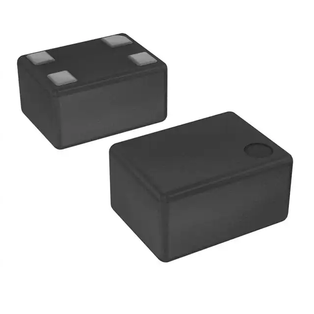
Texas Instruments LMK61E2BBA-SIAR
- Part No.:
- LMK61E2BBA-SIAR
- Manufacturer:
- Texas Instruments
- Category:
- Programmable Oscillators
- Package:
- 8-SMD Module
- Datasheet:
-
 LMK61E2BBA-SIAR.pdf
- Description:
- IC OSC CLOCK 1GHZ 8QFM
- Quantity:
- Payment:

- Shipping:

Inventory:2,739
Please send an inquiry. Send us your inquiry, and we will respond immediately.
Product details
Overview
LMK61E2BBA-SIAR from Texas Instruments is an ultra-low jitter (90 fs RMS typical >100 MHz), programmable oscillator with integrated fractional-N PLL, 4.6–5.6 GHz VCO, and factory-configured 125 MHz LVDS output in a 7 mm × 5 mm QFM-8 package. It features on-chip EEPROM for self-startup, I²C programmability, ±50 ppm total frequency tolerance, and robust –70 dBc PSRR - deployed in FPGA clocking, baseband units, and high-speed serial interface timing.
For engineers reviewing the LMK61E2BBA-SIAR datasheet, LMK61E2BBA-SIAR pinout, LMK61E2BBA-SIAR application, or LMK61E2BBA-SIAR equivalent, key selection criteria include differential output format support (LVDS up to 900 MHz), fine/coarse frequency margining capability, industrial temperature range (–40°C to +85°C), 3.3 V single-supply operation, and EEPROM-based default configuration persistence after power cycle.
Technical Context
The LMK61E2BBA-SIAR implements a fractional-N PLL architecture with integrated 50 MHz crystal reference and VCO spanning 4.6–5.6 GHz, enabling precise synthesis of 125 MHz LVDS output via programmable integer output divider (5–511). Its dual-stage internal LDO regulation isolates analog PLL circuitry from digital noise, achieving –70 dBc PSRR across 50 kHz–1 MHz supply ripple frequencies.
Configuration is performed via I²C interface (100–400 kHz) with open-drain SCL/SDA pins, supporting runtime reprogramming and EEPROM write-back of custom settings. The device supports three differential output formats (LVPECL/LVDS/HCSL), with LVDS mode delivering 300–480 mV differential swing and 45–55% duty cycle at 125 MHz.
Key Specifications
| Parameter | Value and Actual Design Meaning |
|---|---|
| Jitter (RMS) | 90 fs typical (12 kHz–20 MHz), enabling PCIe Gen4/Gen5 and 10G/25G Ethernet timing compliance |
| Output Frequency | 125 MHz LVDS (factory default), user-programmable from 10–900 MHz in LVDS mode |
| Frequency Tolerance | ±50 ppm total (initial + temp + voltage + aging), eliminating need for external calibration |
| PSRR | –70 dBc at 50 kHz–1 MHz, reducing requirement for ultra-low-noise LDOs or extensive board-level filtering |
| VCO Range | 4.6–5.6 GHz, supporting wide output frequency coverage with high phase noise floor suppression |
| Supply Voltage | 3.3 V ±5%, compatible with standard industrial logic rails without level-shifting |
| Operating Temp | –40°C to +85°C, qualified for telecom infrastructure and industrial embedded environments |
| Package | 7 mm × 5 mm QFM-8 (SIA), surface-mount compatible with automated assembly and thermal vias to GND |
Pinout & Package
LMK61E2BBA-SIAR uses a 7 mm × 5 mm, 8-pin QFM (SIA) package with exposed thermal pad connected to GND. Pin 1 is ADD, pin 2 is OUTN, pin 3 is GND, pin 4 is OE, pin 5 is VDD, pin 6 is OUTP, pin 7 is SCL, and pin 8 is SDA - all pins are LVCMOS-compatible except differential outputs (OUTP/OUTN).
| Pin/Terminal | Circuit Role | Design Meaning |
|---|---|---|
| ADD (Pin 1) | I²C address LSB control | Configures I²C target address (00/01/10) by tying to GND/VDD/floating; enables multi-device bus addressing |
| OUTN (Pin 2) | Differential output complement | LVDS-compliant negative output leg; requires 100 Ω termination to VDD/2 for proper common-mode bias |
| GND (Pin 3) | Reference ground | Primary return path for analog/digital supplies and output termination; must connect to low-impedance system GND plane |
| OE (Pin 4) | Output enable input | Active-low control with internal pull-up; asserts high-impedance state on OUTP/OUTN when driven low |
| VDD (Pin 5) | Analog/digital power supply | 3.3 V ±5% input powering PLL, VCO, EEPROM, and output buffers; requires local 10 µF + 100 nF decoupling |
| OUTP (Pin 6) | Differential output true | LVDS-compliant positive output leg; forms 100 Ω differential pair with OUTN for EMI-robust clock distribution |
| SCL (Pin 7) | I²C clock line | Open-drain input requiring external 4.7 kΩ pull-up to VDD; supports 100–400 kHz clock rates for register access |
| SDA (Pin 8) | I²C data line | Open-drain bidirectional input/output requiring same pull-up; carries configuration writes and EEPROM save commands |
Key Features
| Feature | Design Value |
|---|---|
| Ultra-low jitter synthesis | 90 fs RMS typical (12 kHz–20 MHz) enables sub-picosecond timing margins in SerDes receivers |
| Self-starting EEPROM | Factory-programmed 125 MHz LVDS defaults allow immediate operation without host initialization |
| Multi-format output buffer | Single device supports LVPECL (≤1 GHz), LVDS (≤900 MHz), or HCSL (≤400 MHz) - reduces BOM count |
| Fine & coarse margining | I²C-accessible controls adjust output frequency ±100 ppm (fine) or ±1% (coarse) for DVT and compliance testing |
| Integrated power conditioning | On-chip LDOs deliver isolated analog/digital rails, achieving –70 dBc PSRR without external regulators |
| Industrial temperature grade | Validated operation from –40°C to +85°C ensures reliability in base station and network equipment deployments |
Applications
| 10G/25G Ethernet PHY Clocking | FPGA Reference Timing |
|---|---|
Use Scenario: Providing low-jitter reference clock to Ethernet transceivers in switches/routers requiring IEEE 802.3bj/bs compliance. IC Role / Device Role / Timing Role: Primary clock source for PMA blocks, replacing discrete crystal + PLL solutions with integrated jitter performance. Use Value: 90 fs RMS jitter meets <150 fs mask for 25G KR/KP applications, eliminating need for external jitter cleaners. |
Use Scenario: Supplying clean, programmable clock to Xilinx Versal or Intel Agilex FPGAs for high-speed transceiver banks and fabric timing. IC Role / Device Role / Timing Role: Configurable LVDS oscillator enabling dynamic frequency scaling and margining during FPGA bring-up and validation. Use Value: Factory-default 125 MHz LVDS aligns with common GTY/GTP reference requirements; I²C reprogrammability supports multiple design iterations. |
| Baseband Unit (BBU) Timing | Medical Imaging Data Acquisition |
Use Scenario: Generating synchronized clocks for ADC/DAC interfaces and digital front-end processing in 5G NR baseband units. IC Role / Device Role / Timing Role: System-level timing hub distributing phase-aligned clocks to multiple signal chain components. Use Value: ±50 ppm total tolerance and –40°C to +85°C operation ensure long-term stability across outdoor macro cell deployments. |
Use Scenario: Driving high-resolution ADCs in MRI/PET systems where clock-induced spurs degrade SNR and image fidelity. IC Role / Device Role / Timing Role: Ultra-low phase noise oscillator minimizing aperture jitter and harmonic distortion in sampling circuits. Use Value: –162 dBc/Hz phase noise floor at 10 MHz offset (LVDS) suppresses clock-related artifacts in >16-bit medical data converters. |
Equivalent & Alternatives
The following parts are listed as comparable options for similar programmable oscillator applications.
| Alternative Part | Technical Difference | Application Difference | Selection Advice |
|---|---|---|---|
| Si510-125.000M | Fixed-frequency (no I²C), ±20 ppm initial tolerance, 1.8–3.3 V supply, 5×3.2 mm package | Lacks frequency margining and EEPROM programmability; suited for cost-sensitive, static-clock designs | Select when design requires guaranteed 125 MHz only and no field reconfiguration |
| LMK61E0M-125M00 | Same family, lower-jitter variant (75 fs RMS), but fixed 125 MHz LVDS output and no I²C interface | No runtime programming or EEPROM customization; optimized purely for lowest possible jitter at 125 MHz | Select when absolute minimum jitter is critical and flexibility is not required |
Compared with Si510-125.000M and LMK61E0M-125M00, LMK61E2BBA-SIAR uniquely balances programmability, margining, and ultra-low jitter - making it optimal for development-phase systems requiring iterative clock tuning and production-phase designs needing field-upgradable timing.
Availability
LMK61E2BBA-SIAR is available at Aetrix Electronics and suitable for FPGA reference timing, 5G baseband unit synchronization, and high-speed data acquisition systems requiring stable component supply, long-lifecycle availability, and traceable sourcing.
Supply support for LMK61E2BBA-SIAR includes scheduled delivery planning, volume procurement assistance, BOM continuity management, traceable sourcing, and lifecycle availability coordination for OEM customers, industrial embedded developers, connected-device designers, and electronics production programs.
Manufacturer
Texas Instruments is a global semiconductor company specializing in analog, embedded processing, and clock solutions, with over 50 years of leadership in precision timing and power management ICs.
The LMK61E2 series belongs to TI's high-performance programmable oscillator product line, designed specifically for applications demanding ultra-low jitter, flexible output formats, and EEPROM-based configuration persistence in telecom, computing, and test equipment.
FAQ
What is the factory-default output configuration for LMK61E2BBA-SIAR?
The LMK61E2BBA-SIAR ships with factory-programmed EEPROM settings generating 125 MHz LVDS output. This configuration powers up automatically without host intervention, using internal 50 MHz crystal reference and fractional-N PLL with integer output divider set to 40. The device remains in LVDS mode until reconfigured via I²C.
Can LMK61E2BBA-SIAR be used in LVPECL mode, and what are the layout requirements?
Yes - LMK61E2BBA-SIAR supports LVPECL mode up to 1 GHz via I²C register configuration. Layout requires 150 Ω AC-coupled termination to VCC–2 V on each output (OUTP/OUTN), strict 100 Ω differential impedance routing, and separation from noisy digital traces. The 7 mm × 5 mm QFM package's exposed thermal pad must be soldered to a solid GND plane with ≥3 thermal vias.
How does the frequency margining function work, and what is its resolution?
Frequency margining operates in two modes: coarse margining adjusts the output divider value (±1% step size), while fine margining tunes the fractional-N feedback divider numerator (±100 ppm resolution). Both are controlled via dedicated I²C registers and retain settings in EEPROM. Margining is used during DVT for timing closure verification and standards compliance testing.
Is external crystal required for LMK61E2BBA-SIAR operation?
No - the LMK61E2BBA-SIAR integrates a 50 MHz fundamental-mode quartz crystal within the package. This eliminates external crystal placement, matching network design, and associated layout sensitivity, reducing bill-of-materials and improving startup reliability across temperature and vibration conditions.
LMK61E2BBA-SIAR Specifications
- Product attributes
- Attribute value
- Manufacturer:
- Texas Instruments
- Package/Case:
- 8-SMD Module
- Series:
- LMK61E2
- Packaging:
- Tape & Reel (TR)
- Product Status:
- Active
- Base Resonator:
- Silicon
- Type:
- VCXO
- Programmable Type:
- Factory-Configured
- Available Frequency Range:
- 10 MHz ~ 1 GHz
- Function:
- Enable/Disable
- Output:
- HCSL, LVDS, LVPECL
- Voltage - Supply:
- 3.3V
- Frequency Stability:
- -
- Frequency Stability (Total):
- ±50ppm
- Operating Temperature:
- -40°C ~ 85°C
- Spread Spectrum Bandwidth:
- -
- Current - Supply (Max):
- 208mA
- Ratings:
- -
- Mounting Type:
- Surface Mount
- Supplier Device Package:
- 8-QFM (7x5)
- Size / Dimension:
- 0.276" L x 0.197" W (7.00mm x 5.00mm)
- Height - Seated (Max):
- 0.045" (1.15mm)
LMK61E2BBA-SIAR FAQ
1.How can I place an order for LMK61E2BBA-SIAR through Aetrix?
Please submit a Request for Quotation (RFQ) for LMK61E2BBA-SIAR on Aetrix. Our sales agent will provide a competitive quotation and guide you through the order confirmation once you accept the terms.
2.Are the price and stock information for LMK61E2BBA-SIAR reliable?
The price and inventory of LMK61E2BBA-SIAR are updated periodically and may fluctuate due to market conditions. Stock and pricing data are typically refreshed every 24 hours. Quotation validity for LMK61E2BBA-SIAR is usually 5 days.
3.What payment methods are accepted for LMK61E2BBA-SIAR?
We accept Wire Transfer, PayPal, Credit Card, Western Union, MoneyGram, and Escrow for LMK61E2BBA-SIAR transactions.
Note: Certain payment methods may incur a processing fee.
4.How is shipping managed for LMK61E2BBA-SIAR?
LMK61E2BBA-SIAR orders can be shipped via leading logistics carriers, including DHL, UPS, FedEx, TNT, or Registered Mail.
Once your LMK61E2BBA-SIAR order is processed, you will receive an email with the shipment details and tracking number.
Note: Tracking information may take up to 24 hours to appear. Express delivery typically takes 3–5 business days.
5.How can I obtain technical support or documentation for LMK61E2BBA-SIAR?
For technical support, including LMK61E2BBA-SIAR datasheets, pinout diagrams, or application guidance, please contact our engineering support team. They can provide detailed documentation and assistance for your LMK61E2BBA-SIAR requirements.
6.How does Aetrix verify that LMK61E2BBA-SIAR is sourced from the original manufacturer or authorized distributors?
All LMK61E2BBA-SIAR products on Aetrix are procured from qualified distributors and authorized channels. Our dedicated quality assurance team conducts strict verification, including traceability checks and, if necessary, third-party testing. This ensures that LMK61E2BBA-SIAR meets industry standards.
7.What is the process for return or replacement of LMK61E2BBA-SIAR?
All LMK61E2BBA-SIAR units undergo pre-shipment inspection (PSI). If there is an issue with LMK61E2BBA-SIAR, returns or replacements are accepted under the following conditions:
1.Quantity discrepancies, incorrect items, or visible external defects (such as breakage or corrosion), acknowledged by Aetrix.
2.The issue is reported within 90 days of delivery.
3.The LMK61E2BBA-SIAR part is unused and in its original packaging.
Return procedure for LMK61E2BBA-SIAR:
1.Submit a request within 90 days.
2.Obtain a Return Material Authorization (RMA) from Aetrix.
LMK61E2BBA-SIAR Tags
-
LMK61E2-SIAT
Texas Instruments
-
DSC8001CL5
Microchip Technology
-
LMK61E2BBA-SIAT
Texas Instruments
-
LMK61E2BAA-SIAT
Texas Instruments
-
DSC8001BL2
Microchip Technology
-7.00-mm-x-5.00-mm.jpg)
-
DSC1101NL3-PROGT
Microchip Technology
-
DSC8001AL2
Microchip Technology
-
DSC8101CI5
Microchip Technology
-
DSC8121AM2
Microchip Technology
-
DSC8123CI5
Microchip Technology
-
DSC6003HA3B-PROGT
Microchip Technology
-
DSC6101HA3B-PROGT
Microchip Technology
Tech Hub

Jumper cables guide covering safe connection order, red and black clamp placement, final ground connection, cable gauge, length, clamp quality, copper vs CCA cables, jump starter comparison and battery…

LDO regulator guide covering low dropout voltage, power dissipation, thermal design, PSRR, output noise, capacitor stability, adjustable LDO circuits, LDO vs buck converter and datasheet selection chec…

Conditional Access Module guide covering CAM meaning, CI/CI+ interface, smart card authorization, DVB security workflow, TV and set-top box compatibility, internal electronics, ESD protection, connecto…

Guide to electronic component obsolescence covering EOL risk, PCN/PDN notices, last-time buy planning, replacement options, form-fit-function validation, counterfeit risk and BOM lifecycle management.

18650 battery guide covering lithium-ion cell basics, 3.6V/3.7V voltage, 4.2V charging, mAh and Wh capacity, protected cells, chargers, BMS, series-parallel packs, holders, welding and sourcing checks.…

Hall effect sensor guide covering working principle, linear and digital sensors, Arduino circuits, current sensing, speed detection, automotive applications, A3144 examples, signal filtering and datash…

Product Change Notification guide for electronic components, covering PCN meaning, PCN vs PDN/EOL, common change types, risk levels, form-fit-function review, engineering validation, BOM control, LTB/L…

A practical guide to blend door actuators, covering HVAC function, symptoms, location, AC and heater issues, reset and calibration, replacement cost, electrical diagnosis, compatibility checks, and rep…

Engineering guide to Raspberry Pi alternatives, covering chip-level differences, Orange Pi, ROCK, Jetson, Banana Pi, NanoPi, Compute Module, Pico, GPIO, camera, HAT compatibility, and replacement risks…

Engineering guide to dynamic load response testing for high-current buck converters, covering load step setup, slew rate, Vcore undershoot, overshoot, recovery time, probe location, output capacitors a…


