
 My Inquiry
 My Account


Texas Instruments LP2995MRX/NOPB
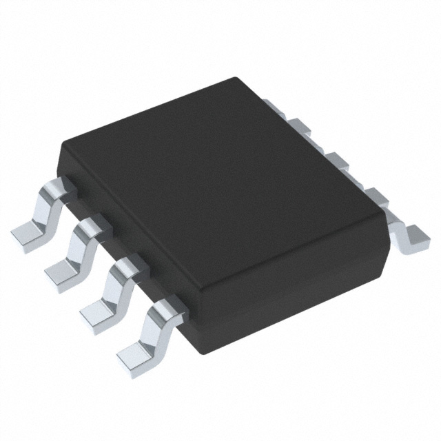
- Part No.:
- LP2995MRX/NOPB
- Manufacturer:
- Texas Instruments
- Category:
- Power Management - Specialized
- Package:
- 8-PowerSOIC (0.154", 3.90mm Width)
- Datasheet:
-
 LP2995MRX/NOPB.pdf
- Description:
- IC REGULATOR DDR TERM 8SOPWRPAD
- Quantity:
- Payment:

- Shipping:

Inventory:5,541
Please send an inquiry. Send us your inquiry, and we will respond immediately.
Product details
Overview
LP2995MRX/NOPB from Texas Instruments is a linear DDR termination regulator designed for SSTL-2 and SSTL-3 bus termination in DDR-SDRAM systems. It sources and sinks up to ±1.5A continuous current, regulates VTT to VDDQ/2 (e.g., 1.25V at VDDQ = 2.5V), and provides a buffered VREF output with ±15mV offset. It operates across 0°C to +125°C and supports remote sensing via VSENSE for improved load regulation on memory buses.
For engineers reviewing the LP2995MRX/NOPB datasheet, LP2995MRX/NOPB pinout, LP2995MRX/NOPB application, or LP2995MRX/NOPB equivalent, this page delivers verified specifications, SO PowerPAD-8 package details, VTT/VREF tracking behavior, thermal derating guidance, and validated alternatives for DDR termination design validation and BOM optimization.
Technical Context
The LP2995MRX/NOPB integrates two high-speed op-amps: one generates VREF as a buffered VDDQ/2 reference, the other drives VTT with shoot-through prevention. Its dual-input architecture separates AVIN (control circuitry) and PVIN (power stage rail), enabling optimized noise isolation and thermal management in DDR memory subsystems.
VTT regulation uses VSENSE for remote feedback, reducing IR drop across long termination planes. Internal 50kΩ resistor dividers fix VTT = VREF = VDDQ/2 by default, but external resistors on VDDQ or VSENSE allow scaling to SSTL-3 (e.g., VDDQ × 0.45) or custom VTT offsets without affecting VREF.
Key Specifications
| Parameter | Value and Actual Design Meaning |
|---|---|
| VTT Output Voltage | 1.25V nominal (VDDQ/2); tracks VDDQ precisely for JEDEC-compliant SSTL-2 termination |
| VTT Offset | ±15 mV max; ensures tight voltage matching between VTT and VREF under zero-load conditions |
| Continuous Current | ±1.5 A; supports sustained sourcing/sinking for DDR-SDRAM I/O bus termination loads |
| Transient Current | ±3 A peak; handles fast DDR data strobe transients without regulation loss |
| Input Voltage Range | AVIN/PVIN: 2.2 V to 5.5 V; enables use with 2.5 V, 3.3 V, or 5 V system rails |
| Thermal Resistance θJA | 43 °C/W (SO PowerPAD-8, JEDEC board); enables higher power dissipation than SOIC-8 (151 °C/W) |
| Quiescent Current | 250–400 µA; low standby draw minimizes impact on system power budget during idle states |
Pinout & Package
LP2995MRX/NOPB is packaged in SO PowerPAD-8 (DDA0008A), featuring an exposed thermal pad (EP) connected to GND for enhanced heat dissipation. The 8-pin layout includes dedicated AVIN, PVIN, VDDQ, VSENSE, VREF, VTT, and dual GND pins - optimized for DDR memory termination layout with minimized loop inductance and thermal resistance.
| Pin/Terminal | Circuit Role | Design Meaning |
|---|---|---|
| 1 (NC) | No internal connection | May be used for thermal vias; no electrical function |
| 2 (GND) | Ground reference | Primary analog ground return for control circuitry |
| 3 (VSENSE) | Remote feedback input | Enables precise VTT regulation at bus midpoint, compensating for PCB trace IR drop |
| 4 (VREF) | Buffered reference output | Provides stable VDDQ/2 (e.g., 1.25V) to chipset and DIMM for global timing reference |
| 5 (VDDQ) | Reference voltage source | Input that sets internal VREF/VTT ratio; must match DDR memory supply rail |
| 6 (AVIN) | Analog supply input | Powers op-amps and reference circuitry; tied to PVIN for SSTL-2 simplicity |
| 7 (PVIN) | Power supply input | Drives VTT output stage; separate from AVIN to isolate noise-sensitive analog paths |
| 8 (VTT) | Termination voltage output | Regulated output sourcing/sinking ±1.5A; connects directly to DDR bus termination resistors |
| EP (Exposed Pad) | Thermal ground | Must be soldered to PCB ground plane with ≥6 thermal vias for θJA = 43 °C/W performance |
Key Features
| Feature | Design Value |
|---|---|
| Source/sink capability | ±1.5A continuous, ±3A transient - meets DDR-SDRAM dynamic termination current demands |
| VTT–VREF tracking | ±15mV offset ensures SSTL-2 compliance and eliminates reference mismatch errors |
| VSENSE remote sensing | Compensates for >50 mV IR drop across 6-inch VTT planes, maintaining <1% regulation error at load |
| Dual-rail inputs (AVIN/PVIN) | Reduces noise coupling into reference path; allows independent bypassing for EMI-sensitive designs |
| No external resistors required | Internal 50kΩ divider sets VTT = VREF = VDDQ/2 - simplifies layout and reduces BOM count |
Applications
| DDR-SDRAM Memory Modules | SSTL-2 Compliant Systems |
|---|---|
Use Scenario: Termination of bidirectional data/address/control lines on 168-pin or 240-pin DDR SDRAM DIMMs in desktop/server motherboards. IC Role / Device Role / Timing Role: Provides active VTT termination voltage and global VREF reference synchronized to VDDQ rail. Use Value: Eliminates signal reflections at >133 MHz clock rates by maintaining precise 1.25V termination with <±15mV drift over temperature and load. | Use Scenario: Chipset-to-memory interface in Intel Pentium 4 or AMD Athlon XP platforms requiring JEDEC SSTL-2 Class II parallel termination. IC Role / Device Role / Timing Role: Regulates VTT to exactly half the VDDQ supply while buffering VREF for Northbridge and memory controller reference inputs. Use Value: Ensures setup/hold timing margins remain intact across 0–125°C by tracking VDDQ/2 with <0.5% load regulation error. |
| SSTL-3 Compatible Designs | DDR Bus Remote Sensing |
Use Scenario: Upgraded DDR systems using 3.3V VDDQ rails where VTT must be set to 1.5V (SSTL-3) instead of 1.25V (SSTL-2). IC Role / Device Role / Timing Role: External resistor on VDDQ pin scales internal divider to generate VTT = VDDQ × 0.45, decoupling VREF from VTT adjustment. Use Value: Enables single-component migration from SSTL-2 to SSTL-3 without redesigning reference distribution network. | Use Scenario: High-density server memory subsystems with >12-inch VTT routing where trace resistance causes >80mV voltage drop at full load. IC Role / Device Role / Timing Role: VSENSE pin connected to center of termination bus enables closed-loop regulation at point-of-load. Use Value: Reduces worst-case VTT deviation from ±8% (local sense) to ±0.3% (remote sense), preventing data eye closure. |
Equivalent & Alternatives
The following parts are listed as comparable options for similar DDR termination regulator applications.
| Alternative Part | Technical Difference | Application Difference | Selection Advice |
|---|---|---|---|
| LP2996MRX/NOPB | Higher continuous current (±2A), lower quiescent current (180µA), same SO PowerPAD-8 package | Supports DDR2 systems with tighter VTT tolerance (±10mV) and extended temperature range (−40°C to +125°C) | Select when upgrading to DDR2 or requiring lower IQ and tighter regulation |
| TPS51100DGQR | Switching architecture (90% efficiency), 3A continuous, integrated MOSFETs, requires external compensation | Replaces linear regulators in thermally constrained DDR3/LPDDR2 designs where power loss exceeds 1.5W | Select when thermal budget is limited and board space allows switching noise filtering |
Compared with LP2995MRX/NOPB, LP2996MRX/NOPB offers tighter VTT regulation and lower IQ for next-gen DDR, while TPS51100DGQR replaces linear topology with switching efficiency for high-current DDR3 applications - neither is pin-compatible, requiring layout revision.
Availability
LP2995MRX/NOPB is available at Aetrix Electronics and suitable for DDR-SDRAM termination, SSTL-2 compliant memory interfaces, and DDR bus remote sensing applications requiring stable component supply and long-term industrial availability.
Supply support for LP2995MRX/NOPB includes scheduled delivery planning, volume procurement assistance, BOM continuity management, traceable sourcing, and lifecycle availability coordination for OEM customers, industrial embedded developers, connected-device designers, and electronics production programs.
Manufacturer
Texas Instruments is a global semiconductor leader specializing in analog, embedded processing, and logic technologies, with decades of expertise in power management and interface solutions.
The LP2995MRX/NOPB belongs to TI's DDR termination regulator product line, engineered specifically to meet JEDEC SSTL-2/SSTL-3 specifications for reliable, low-noise memory bus termination in computing and communications infrastructure.
FAQ
What is the maximum continuous output current rating for LP2995MRX/NOPB?
The LP2995MRX/NOPB supports ±1.5A continuous sourcing and sinking current at VTT. This rating assumes proper thermal management - specifically, mounting on a 4-layer PCB with ≥6 thermal vias to the ground plane and airflow ≥200 LFPM. Exceeding this current without derating risks junction temperature exceeding 125°C, triggering thermal shutdown. Peak transient capability reaches ±3A for ≤10ms pulses.
How does LP2995MRX/NOPB achieve VTT–VREF tracking, and what is its typical accuracy?
LP2995MRX/NOPB achieves VTT–VREF tracking through matched internal resistor dividers and shared reference architecture. VREF is a buffered copy of VDDQ/2, and VTT is regulated to match it using a high-gain error amplifier. Electrical Characteristics specify VOSVTT (VTT offset vs VREF) as ±15mV over 0°C to +125°C - ensuring <1.2% tracking error at 1.25V nominal, critical for SSTL-2 compliance.
Can LP2995MRX/NOPB be used for SSTL-3 termination, and how is the reference voltage adjusted?
Yes, LP2995MRX/NOPB supports SSTL-3 by modifying the internal VDDQ divider ratio. Adding an 11.1kΩ resistor in series with the VDDQ pin changes the effective divider to yield VTT = VDDQ × 0.45 (e.g., 1.5V at 3.3V VDDQ). VREF remains at VDDQ/2 unless similarly modified; the datasheet confirms this scaling method preserves regulation stability and transient response within specified limits.
What is the role of the VSENSE pin on LP2995MRX/NOPB, and how should it be connected?
The VSENSE pin on LP2995MRX/NOPB provides remote feedback for improved load regulation. It should be connected to the midpoint of the VTT termination bus - typically at the center of the DDR memory channel - to compensate for IR drop across PCB traces. If remote sensing is unused, VSENSE must still be shorted to VTT per datasheet requirement to maintain regulation integrity and prevent instability.
What thermal considerations apply to LP2995MRX/NOPB in SO PowerPAD-8 package?
LP2995MRX/NOPB in SO PowerPAD-8 has θJA = 43°C/W on a JEDEC-standard board. To avoid exceeding 125°C junction temperature, maximum power dissipation must be limited: PDmax = (125°C − TA)/43°C/W. At 70°C ambient, PDmax = 1.28W. Since P = (VIN − VOUT) × IOUT, operation at PVIN = 2.5V and VTT = 1.25V delivering 1.5A yields 1.875W - requiring additional airflow or copper area to stay within safe thermal limits.
LP2995MRX/NOPB Specifications
- Product attributes
- Attribute value
- Manufacturer:
- Texas Instruments
- Series:
- -
- Package/Case:
- 8-PowerSOIC (0.154", 3.90mm Width)
- Packaging:
- Tape & Reel (TR)
- Product Status:
- Active
- Applications:
- DDR Terminator
- Current - Supply:
- 250µA
- Voltage - Supply:
- 2.2V ~ 5.5V
- Operating Temperature:
- 0°C ~ 125°C
- Grade:
- -
- Qualification:
- -
- Mounting Type:
- Surface Mount
- Supplier Device Package:
- 8-SO PowerPad
LP2995MRX/NOPB FAQ
1.How can I place an order for LP2995MRX/NOPB through Aetrix?
Please submit a Request for Quotation (RFQ) for LP2995MRX/NOPB on Aetrix. Our sales agent will provide a competitive quotation and guide you through the order confirmation once you accept the terms.
2.Are the price and stock information for LP2995MRX/NOPB reliable?
The price and inventory of LP2995MRX/NOPB are updated periodically and may fluctuate due to market conditions. Stock and pricing data are typically refreshed every 24 hours. Quotation validity for LP2995MRX/NOPB is usually 5 days.
3.What payment methods are accepted for LP2995MRX/NOPB?
We accept Wire Transfer, PayPal, Credit Card, Western Union, MoneyGram, and Escrow for LP2995MRX/NOPB transactions.
Note: Certain payment methods may incur a processing fee.
4.How is shipping managed for LP2995MRX/NOPB?
LP2995MRX/NOPB orders can be shipped via leading logistics carriers, including DHL, UPS, FedEx, TNT, or Registered Mail.
Once your LP2995MRX/NOPB order is processed, you will receive an email with the shipment details and tracking number.
Note: Tracking information may take up to 24 hours to appear. Express delivery typically takes 3–5 business days.
5.How can I obtain technical support or documentation for LP2995MRX/NOPB?
For technical support, including LP2995MRX/NOPB datasheets, pinout diagrams, or application guidance, please contact our engineering support team. They can provide detailed documentation and assistance for your LP2995MRX/NOPB requirements.
6.How does Aetrix verify that LP2995MRX/NOPB is sourced from the original manufacturer or authorized distributors?
All LP2995MRX/NOPB products on Aetrix are procured from qualified distributors and authorized channels. Our dedicated quality assurance team conducts strict verification, including traceability checks and, if necessary, third-party testing. This ensures that LP2995MRX/NOPB meets industry standards.
7.What is the process for return or replacement of LP2995MRX/NOPB?
All LP2995MRX/NOPB units undergo pre-shipment inspection (PSI). If there is an issue with LP2995MRX/NOPB, returns or replacements are accepted under the following conditions:
1.Quantity discrepancies, incorrect items, or visible external defects (such as breakage or corrosion), acknowledged by Aetrix.
2.The issue is reported within 90 days of delivery.
3.The LP2995MRX/NOPB part is unused and in its original packaging.
Return procedure for LP2995MRX/NOPB:
1.Submit a request within 90 days.
2.Obtain a Return Material Authorization (RMA) from Aetrix.
LP2995MRX/NOPB Tags

-
TPS2511DGNR
Texas Instruments

-
UTC2000/MG
Microchip Technology

-
TUSB320HAIRWBR
Texas Instruments

-
TPS61252DSGR
Texas Instruments

-
PI5USB30216CXUAEX
Diodes Incorporated

-
SN6501DBVR
Texas Instruments

-
CYPD3177-24LQXQT
Infineon Technologies
-
SN6501QDBVRQ1
Texas Instruments

-
STUSB1600AQTR
STMicroelectronics

-
SN6505BDBVR
Texas Instruments
-
SN6501DBVT
Texas Instruments

-
TPS65150PWPR
Texas Instruments
Tech Hub

A practical engineering guide to 3.3V and 5V logic compatibility, input thresholds, resistor dividers, translator ICs, MOSFET level shifting, I2C pull-ups, timing limits and power-sequencing risks.

The 74HC595 uses push-pull logic outputs, while the TPIC6B595 uses 50 V open-drain DMOS sinks for higher-power loads. This guide compares timing, current limits, 3.3 V interfacing, load wiring, thermal…

The 74HC595 converts serial data into eight stable parallel outputs. This guide covers pin functions, shift and storage timing, OE and MR behavior, drive-current limits, cascading, voltage compatibilit…

A technical comparison of level-sensitive latches and edge-triggered flip-flops, covering timing windows, setup and hold limits, master–slave operation, time borrowing, race-through, HDL inference and…

A D latch stores one bit while Enable controls when data can pass. This reference covers gate-level operation, truth tables, transparency, setup and hold timing, LE versus OE, common ICs and practical …

An SR latch stores one bit through cross-coupled feedback. This engineering reference covers NOR and NAND implementations, truth tables, forbidden-state recovery, gated operation, switch debouncing, fa…

Latch circuits retain one bit through feedback. This technical reference covers SR and D latches, truth tables, transparency, timing limits, latch-versus-flip-flop behavior, applications and common log…

An engineering guide to LED driver operation, constant-current and constant-voltage outputs, linear and switching topologies, dimming, IC selection, calculations, replacement compatibility, and fault c…

Operational amplifier guide covering op amp basics, feedback, ideal vs real op amps, common configurations, buffer circuits, offset, bias current, gain-bandwidth, slew rate, rail-to-rail limits and sel…

Jumper cables guide covering safe connection order, red and black clamp placement, final ground connection, cable gauge, length, clamp quality, copper vs CCA cables, jump starter comparison and battery…


