
 My Inquiry
 My Account


Analog Devices Inc. LTC4360CSC8-1#TRMPBF
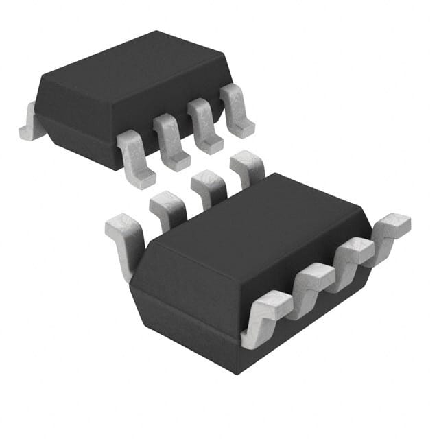
- Part No.:
- LTC4360CSC8-1#TRMPBF
- Manufacturer:
- Analog Devices Inc.
- Category:
- Power Management - Specialized
- Package:
- 8-VFSOP (0.049", 1.25mm Width)
- Datasheet:
-
 LTC4360CSC8-1#TRMPBF.pdf
- Description:
- IC OVERVOLTAGE PROT CONT SC70-8
- Quantity:
- Payment:

- Shipping:

Inventory:584
Please send an inquiry. Send us your inquiry, and we will respond immediately.
Product details
Overview
LTC4360CSC8-1#TRMPBF from Analog Devices is an overvoltage protection controller designed to safeguard 2.5V–5.5V portable systems using external N-channel MOSFETs. It features a 5.8V ±2% overvoltage threshold, sub-1µs turn-off response, and integrated dV/dt-controlled gate ramp-up for inrush current limiting-enabling robust USB, wall adaptor, and car battery input protection in smartphones and MP3 players.
For engineers reviewing the LTC4360CSC8-1#TRMPBF datasheet, LTC4360CSC8-1#TRMPBF pinout, LTC4360CSC8-1#TRMPBF application, or LTC4360CSC8-1#TRMPBF equivalent, this device delivers precise 5.8V overvoltage detection, soft-start control via GATE pin ramping, low-current shutdown (1.5µA) when ON is high, and power-good monitoring via open-drain PWRGD with 65ms assertion delay.
Technical Context
The LTC4360CSC8-1#TRMPBF implements a fast analog overvoltage comparator with 25–300mV hysteresis and a charge-pump-based gate driver that delivers ≥4.5V gate overdrive above VOUT for logic-level N-MOSFETs. Its internal 130ms start-up delay prevents false triggering during input transients, while the GATE pin's 3V/ms controlled ramp limits inrush current into downstream capacitance.
It uses an active-low ON pin to enable/disable operation and enter 1.5µA sleep mode; during sleep, GATE is weakly pulled low (40µA), ensuring gentle MOSFET turn-off without voltage spikes. The PWRGD output asserts low only after GATE exceeds its 5.7–7.8V threshold for ≥65ms, providing reliable power sequencing feedback.
Key Specifications
| Parameter | Value and Actual Design Meaning |
|---|---|
| Overvoltage Threshold | 5.8V ±2% - enables accurate clamping before downstream ICs exceed absolute max ratings |
| Turn-Off Propagation Delay | <1µs - isolates load within one microsecond of overvoltage detection |
| Input Voltage Range | 2.5V to 80V - supports wide-input portable power sources including 24V adaptors and automotive transients |
| Gate Drive Capability | ≥4.5V above VOUT at VIN ≥3V - ensures full enhancement of logic-level N-MOSFETs like Si1470DH |
| Quiescent Current (ON = 2.5V) | 1.5µA - enables ultra-low-power sleep mode for battery-backed systems |
| PWRGD Assertion Delay | 65ms after GATE > VGATE(TH) - provides stable power-good signal only after regulated output is established |
| Start-Up Delay | 130ms - prevents false triggering during hot-plug or cable inductive overshoot |
Pinout & Package
Package: 8-Lead Plastic SC70 (SC8), 0°C to 70°C operating temperature range, 2.2mm × 1.35mm footprint.
| Pin/Terminal | Circuit Role | Design Meaning |
|---|---|---|
| IN | Supply Input Voltage Sense | Monitors input for overvoltage (5.8V threshold); withstands up to 80V transient |
| GND (Pins 2,3,4) | Ground Reference | Three dedicated ground pins minimize impedance and improve noise immunity |
| GATE | N-MOSFET Gate Driver Output | Drives external N-channel MOSFET gate with 3V/ms ramp and 30mA fast pull-down |
| OUT | Output Voltage Sense | Connects to MOSFET source to set GATE-to-OUT clamp voltage (6V max differential) |
| ON | Active-Low Enable Input | Drives low to enable; high forces 1.5µA sleep mode and gradual MOSFET turn-off |
| PWRGD | Power-Good Status Output | Open-drain output with 500kΩ pull-up to OUT; pulls low after 65ms stable gate voltage |
Key Features
| Feature | Design Value |
|---|---|
| No TVS or input capacitor required | 80V overvoltage tolerance and internal clamping eliminate need for external transient suppressors in most designs |
| Adjustable inrush control | GATE ramp rate set by internal 3V/ms or external capacitor (CG = 10µA × COUT / IINRUSH) |
| Gentle shutdown on ON high | 40µA weak pull-down on GATE avoids abrupt current interruption and minimizes input voltage transients |
| Accurate power sequencing | PWRGD asserts only after sustained GATE voltage > VGATE(TH), preventing premature system wake-up |
| Low-impedance ground path | Three GND pins reduce thermal resistance (θJA = 270°C/W) and improve EMI performance |
Applications
| USB Power Input Protection | Smartphone Charging Circuit |
|---|---|
Use Scenario: USB port subjected to misconnected 12V wall adaptor or hot-plug inductive overshoot. IC Role / Device Role / Timing Role: Overvoltage controller that senses IN voltage and disables N-MOSFET pass element within 1µs. Use Value: Prevents damage to 3.3V/1.8V baseband and application processors by limiting VOUT rise to ≤1V during 20V transients. |
Use Scenario: Dual-input mobile phone accepting power from USB (5V) and car charger (12V) simultaneously. IC Role / Device Role / Timing Role: Primary overvoltage guard upstream of PMIC; coordinates with ON pin for system-initiated power-down. Use Value: Enables 1.5µA sleep mode during standby, extending battery life while maintaining fast (<130ms) reactivation on plug-in. |
| MP3/MP4 Player Power Management | Digital Camera Battery Charging Interface |
Use Scenario: Portable media player powered via generic AC adaptor with poor regulation causing 6.2V DC overvoltage. IC Role / Device Role / Timing Role: Precision 5.8V threshold detector with 25–300mV hysteresis to avoid oscillation near trip point. Use Value: Rejects marginal overvoltages without nuisance shutdowns while guaranteeing protection at worst-case 5.916V. |
Use Scenario: Camera with Li-ion battery charging circuit exposed to reverse-polarity or 24V surge from faulty dock. IC Role / Device Role / Timing Role: Front-end protector controlling N-MOSFET pass device; works with external clamp diodes for polarity safety. Use Value: Absorbs single-pulse energy (≤16µJ) from cable inductance without requiring TVS, reducing BOM count and board area. |
Equivalent & Alternatives
The following parts are listed as comparable options for similar overvoltage protection applications.
| Alternative Part | Technical Difference | Application Difference | Selection Advice |
|---|---|---|---|
| LTC4360CSC8-2#TRMPBF | Includes GATEP pin for driving external P-MOSFET; adds negative voltage protection capability | Required where input may experience reverse polarity (e.g., docking stations with bidirectional ports) | Select LTC4360CSC8-2#TRMPBF only if negative voltage protection is needed; LTC4360CSC8-1#TRMPBF offers lower cost and simpler layout for unidirectional inputs |
| LT4356-1IMS#PBF | Wider input range (4V–80V), adjustable OVP threshold (1.2V–18V), reverse input protection to –60V | Suitable for industrial 24V/48V systems; lacks integrated soft-start dV/dt control and low-current sleep mode | Choose LT4356-1IMS#PBF for programmable thresholds and harsher environments; LTC4360CSC8-1#TRMPBF better fits compact, battery-sensitive consumer devices |
Compared with LTC4360CSC8-2#TRMPBF, the LTC4360CSC8-1#TRMPBF omits GATEP and negative voltage protection but achieves 1.5µA shutdown current and tighter 5.8V threshold accuracy-making it optimal for space-constrained, single-polarity USB-powered devices. Versus LT4356-1IMS#PBF, it trades programmability for lower quiescent current and integrated inrush control, simplifying design for portable 5V systems.
Availability
LTC4360CSC8-1#TRMPBF is available at Aetrix Electronics and suitable for USB protection, smartphone charging circuits, and MP3/MP4 player power management requiring stable component supply across high-volume consumer electronics production.
Supply support for LTC4360CSC8-1#TRMPBF includes scheduled delivery planning, volume procurement assistance, BOM continuity management, traceable sourcing, and lifecycle availability coordination for OEM customers, industrial embedded developers, connected-device designers, and electronics production programs.
Manufacturer
Analog Devices is a global leader in high-performance analog, mixed-signal, and digital signal processing semiconductors, serving precision instrumentation, communications, and industrial markets since 1965.
The LTC4360 product line was developed specifically for overvoltage protection in portable electronics with multiple input sources, emphasizing fast response, minimal external components, and ultra-low quiescent current in miniature SC70 packages.
FAQ
What is the overvoltage threshold accuracy of the LTC4360CSC8-1#TRMPBF?
The LTC4360CSC8-1#TRMPBF features a 5.8V overvoltage threshold with ±2% accuracy over the full 0°C to 70°C operating temperature range. This corresponds to a guaranteed trip window of 5.684V to 5.916V, enabling reliable protection of 3.3V and 5V logic without nuisance shutdowns or unsafe delays. The threshold is internally trimmed and does not require external calibration.
How does the LTC4360CSC8-1#TRMPBF handle inrush current during power-up?
The LTC4360CSC8-1#TRMPBF controls inrush current by ramping the GATE pin voltage at 3V/ms, resulting in a predictable dV/dt-limited output voltage rise. For a 10µF output capacitor, this yields ~30mA inrush current. An external capacitor from GATE to GND allows further reduction-e.g., a 33nF capacitor lowers ramp rate to ~0.3V/ms, cutting inrush proportionally. No external compensation is needed in standard configurations.
Can the LTC4360CSC8-1#TRMPBF be used with P-channel MOSFETs?
No-the LTC4360CSC8-1#TRMPBF is designed exclusively to drive external N-channel MOSFETs via its GATE pin. It lacks the GATEP pin found on the LTC4360-2 variant, which is required to control P-channel devices for negative voltage protection. Attempting to drive a P-MOSFET with the LTC4360CSC8-1#TRMPBF will result in incorrect biasing and failure to achieve proper overvoltage isolation.
What is the function of the ON pin on the LTC4360CSC8-1#TRMPBF?
The ON pin on the LTC4360CSC8-1#TRMPBF is an active-low enable input with internal 5µA pull-down. When held low, the device operates normally; when driven high, it enters a 1.5µA sleep mode and gently turns off the external N-MOSFET using a 40µA weak pull-down on GATE. This feature enables system-controlled power gating without external FETs or complex sequencing logic.
Does the LTC4360CSC8-1#TRMPBF require external components for basic overvoltage protection?
No-basic overvoltage protection with the LTC4360CSC8-1#TRMPBF requires only an external N-channel MOSFET (e.g., Si1470DH) and output capacitor. The device integrates the overvoltage comparator, gate driver, charge pump, and PWRGD monitor, eliminating the need for TVS diodes, input capacitors, or voltage dividers in most applications. Layout best practices (short GND traces, wide power paths) are the only additional requirements.
LTC4360CSC8-1#TRMPBF Specifications
- Product attributes
- Attribute value
- Manufacturer:
- Analog Devices Inc.
- Series:
- -
- Package/Case:
- 8-VFSOP (0.049", 1.25mm Width)
- Packaging:
- Tape & Reel (TR)
- Product Status:
- Active
- Applications:
- Handheld/Mobile Devices
- Current - Supply:
- 220µA
- Voltage - Supply:
- 2.5V ~ 80V
- Operating Temperature:
- 0°C ~ 70°C
- Grade:
- -
- Qualification:
- -
- Mounting Type:
- Surface Mount
- Supplier Device Package:
- SC-70-8
LTC4360CSC8-1#TRMPBF FAQ
1.How can I place an order for LTC4360CSC8-1#TRMPBF through Aetrix?
Please submit a Request for Quotation (RFQ) for LTC4360CSC8-1#TRMPBF on Aetrix. Our sales agent will provide a competitive quotation and guide you through the order confirmation once you accept the terms.
2.Are the price and stock information for LTC4360CSC8-1#TRMPBF reliable?
The price and inventory of LTC4360CSC8-1#TRMPBF are updated periodically and may fluctuate due to market conditions. Stock and pricing data are typically refreshed every 24 hours. Quotation validity for LTC4360CSC8-1#TRMPBF is usually 5 days.
3.What payment methods are accepted for LTC4360CSC8-1#TRMPBF?
We accept Wire Transfer, PayPal, Credit Card, Western Union, MoneyGram, and Escrow for LTC4360CSC8-1#TRMPBF transactions.
Note: Certain payment methods may incur a processing fee.
4.How is shipping managed for LTC4360CSC8-1#TRMPBF?
LTC4360CSC8-1#TRMPBF orders can be shipped via leading logistics carriers, including DHL, UPS, FedEx, TNT, or Registered Mail.
Once your LTC4360CSC8-1#TRMPBF order is processed, you will receive an email with the shipment details and tracking number.
Note: Tracking information may take up to 24 hours to appear. Express delivery typically takes 3–5 business days.
5.How can I obtain technical support or documentation for LTC4360CSC8-1#TRMPBF?
For technical support, including LTC4360CSC8-1#TRMPBF datasheets, pinout diagrams, or application guidance, please contact our engineering support team. They can provide detailed documentation and assistance for your LTC4360CSC8-1#TRMPBF requirements.
6.How does Aetrix verify that LTC4360CSC8-1#TRMPBF is sourced from the original manufacturer or authorized distributors?
All LTC4360CSC8-1#TRMPBF products on Aetrix are procured from qualified distributors and authorized channels. Our dedicated quality assurance team conducts strict verification, including traceability checks and, if necessary, third-party testing. This ensures that LTC4360CSC8-1#TRMPBF meets industry standards.
7.What is the process for return or replacement of LTC4360CSC8-1#TRMPBF?
All LTC4360CSC8-1#TRMPBF units undergo pre-shipment inspection (PSI). If there is an issue with LTC4360CSC8-1#TRMPBF, returns or replacements are accepted under the following conditions:
1.Quantity discrepancies, incorrect items, or visible external defects (such as breakage or corrosion), acknowledged by Aetrix.
2.The issue is reported within 90 days of delivery.
3.The LTC4360CSC8-1#TRMPBF part is unused and in its original packaging.
Return procedure for LTC4360CSC8-1#TRMPBF:
1.Submit a request within 90 days.
2.Obtain a Return Material Authorization (RMA) from Aetrix.
LTC4360CSC8-1#TRMPBF Tags

-
TPS2511DGNR
Texas Instruments

-
UTC2000/MG
Microchip Technology

-
TUSB320HAIRWBR
Texas Instruments

-
TPS61252DSGR
Texas Instruments

-
PI5USB30216CXUAEX
Diodes Incorporated

-
SN6501DBVR
Texas Instruments

-
CYPD3177-24LQXQT
Infineon Technologies
-
SN6501QDBVRQ1
Texas Instruments

-
STUSB1600AQTR
STMicroelectronics

-
SN6505BDBVR
Texas Instruments
-
SN6501DBVT
Texas Instruments

-
TPS65150PWPR
Texas Instruments
Tech Hub

A practical engineering guide to 3.3V and 5V logic compatibility, input thresholds, resistor dividers, translator ICs, MOSFET level shifting, I2C pull-ups, timing limits and power-sequencing risks.

The 74HC595 uses push-pull logic outputs, while the TPIC6B595 uses 50 V open-drain DMOS sinks for higher-power loads. This guide compares timing, current limits, 3.3 V interfacing, load wiring, thermal…

The 74HC595 converts serial data into eight stable parallel outputs. This guide covers pin functions, shift and storage timing, OE and MR behavior, drive-current limits, cascading, voltage compatibilit…

A technical comparison of level-sensitive latches and edge-triggered flip-flops, covering timing windows, setup and hold limits, master–slave operation, time borrowing, race-through, HDL inference and…

A D latch stores one bit while Enable controls when data can pass. This reference covers gate-level operation, truth tables, transparency, setup and hold timing, LE versus OE, common ICs and practical …

An SR latch stores one bit through cross-coupled feedback. This engineering reference covers NOR and NAND implementations, truth tables, forbidden-state recovery, gated operation, switch debouncing, fa…

Latch circuits retain one bit through feedback. This technical reference covers SR and D latches, truth tables, transparency, timing limits, latch-versus-flip-flop behavior, applications and common log…

An engineering guide to LED driver operation, constant-current and constant-voltage outputs, linear and switching topologies, dimming, IC selection, calculations, replacement compatibility, and fault c…

Operational amplifier guide covering op amp basics, feedback, ideal vs real op amps, common configurations, buffer circuits, offset, bias current, gain-bandwidth, slew rate, rail-to-rail limits and sel…

Jumper cables guide covering safe connection order, red and black clamp placement, final ground connection, cable gauge, length, clamp quality, copper vs CCA cables, jump starter comparison and battery…


