
 My Inquiry
 My Account


Analog Devices Inc. LTC4364IDE-1#PBF
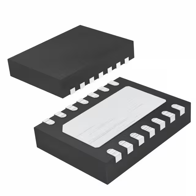
- Part No.:
- LTC4364IDE-1#PBF
- Manufacturer:
- Analog Devices Inc.
- Category:
- Surge Suppression Ics
- Package:
- 14-WFDFN Exposed Pad
- Datasheet:
-
 LTC4364IDE-1#PBF.pdf
- Description:
- IC SURGE STOPPER W/DIODE 14DFN
- Quantity:
- Payment:

- Shipping:

Inventory:507
Please send an inquiry. Send us your inquiry, and we will respond immediately.
Product details
Overview
LTC4364IDE-1#PBF from Analog Devices is a surge stopper with ideal diode controller for automotive and industrial power rail protection. It regulates output voltage to 27V during 92V/1ms transients, provides reverse input protection to –40V, and latches off the external N-channel MOSFET pass device upon overvoltage or overcurrent fault timeout. Used in 12V/24V vehicle electronics requiring AEC-Q100-compliant transient resilience.
For engineers reviewing the LTC4364IDE-1#PBF datasheet, LTC4364IDE-1#PBF pinout, LTC4364IDE-1#PBF application, or LTC4364IDE-1#PBF equivalent, key selection criteria include latch-off behavior (vs auto-retry), 4V–80V operating range, 10μA shutdown current, adjustable fault timer via TMR capacitor, and dual-MOSFET gate drive architecture for surge + reverse polarity protection.
Technical Context
The LTC4364IDE-1#PBF implements two independent control loops: a voltage amplifier regulating HGATE to clamp VOUT at 27V using FB feedback, and a current-sense amplifier limiting ∆VSNS to 50mV (or 25mV during output short) to protect the pass MOSFET. Fault detection uses a single TMR capacitor charged by voltage- or current-dependent current sources - 5× higher pull-up current during overcurrent versus overvoltage to accelerate turn-off.
Its latch-off behavior distinguishes it from the LTC4364-2 variant: after HGATE turns off due to fault timeout, LTC4364IDE-1#PBF holds HGATE low until manually reset via SHDN or UV pin. The ideal diode loop actively controls DGATE to maintain ~30mV forward drop across the second MOSFET, minimizing conduction loss while suppressing reverse current transients during input collapse or short.
Key Specifications
| Parameter | Value and Actual Design Meaning |
|---|---|
| Operating Voltage Range | 4V to 80V input supply; supports cold-crank operation and withstands 200V/1ms transients with VCC clamp |
| Output Clamp Voltage | Adjustable via FB divider; typical 27V clamping during 92V input surge (Figure TA01b) |
| Fault Response | Latch-off: HGATE remains off after fault timeout until SHDN or UV reset; no auto-retry |
| Shutdown Current | 10μA at 12V - enables low-power system standby without compromising surge readiness |
| Reverse Protection | –40V reverse input tolerance; ideal diode loop blocks reverse current with <1.5μs DGATE turn-off delay |
| Package & Temp | 14-lead 4mm × 3mm DFN; rated for –40°C to +85°C ambient (Industrial grade) |
| AEC-Q100 | Qualified per AEC-Q100 Rev H Grade 3 (–40°C to +85°C); suitable for automotive front-end protection |
Pinout & Package
Package: 14-lead (4mm × 3mm) plastic DFN with optional exposed pad (Pin 15) connected to GND. Thermal resistance θJA = 45°C/W.
| Pin/Terminal | Circuit Role | Design Meaning |
|---|---|---|
| OUT (Pin 1) | Output voltage sense input | Senses drain of HGATE-controlled MOSFET; triggers ENOUT high-impedance state when VOUT > VCC − 0.7V |
| SENSE (Pin 2) | Current sense input | Monitors voltage across external sense resistor; sets 50mV (or 25mV) current limit threshold |
| DGATE (Pin 3) | Ideal diode gate drive output | Drives second N-MOSFET; maintains ~30mV forward drop and pulls low within 1.5μs on reverse current |
| SOURCE (Pin 4) | Common source reference | Anode node for ideal diode; return path for HGATE/DGATE charge pumps and sense amplifier |
| HGATE (Pin 5) | Surge stopper gate drive output | Controls main N-MOSFET pass device; regulated to clamp VOUT during overvoltage events |
| VCC (Pin 6) | Positive supply input | Operates from 4V–80V; tolerates –40V reverse bias; powers internal circuitry and gate drivers |
| SHDN (Pin 7) | Shutdown control input | Pull below 0.5V to reduce ICC to 10μA and latch HGATE/DGATE off; resets fault latch |
| UV (Pin 8) | Undervoltage comparator input | 1.25V threshold; pulls HGATE low if violated; 0.6V reset threshold for latch recovery (LTC4364-1 only) |
| OV (Pin 9) | Overvoltage comparator input | 1.25V threshold; inhibits retry during overvoltage; must fall below threshold before HGATE re-enables |
| GND (Pin 10) | Device ground | Reference for all analog circuits and open-drain outputs (FLT, ENOUT) |
| FLT (Pin 11) | Fault indicator output | Open-drain; pulls low at TMR = 1.25V (warning), stays low after HGATE latch-off |
| ENOUT (Pin 12) | Enable output | Open-drain; high-impedance when VOUT > VCC − 0.7V; latched low if VOUT drops below 2.2V |
| TMR (Pin 13) | Fault timer capacitor node | Charged by voltage- or current-dependent current sources; 1.25V = warning, 1.35V = HGATE turn-off |
| FB (Pin 14) | Feedback input | 1.25V internal reference; sets output clamp voltage via resistive divider from OUT to GND |
Key Features
| Feature | Design Value |
|---|---|
| Latch-off fault response | Ensures definitive shutdown during sustained overvoltage (e.g., load dump), preventing MOSFET thermal runaway |
| Integrated ideal diode control | Replaces Schottky with N-MOSFET, reducing forward drop from ~0.4V to ~30mV and eliminating reverse recovery losses |
| Reverse input tolerance to –40V | Enables direct connection to battery terminals without external reverse-blocking diodes or TVS |
| Adjustable fault timer | Single external capacitor sets warning (1.25V), turn-off (1.35V), and cool-down (32-cycle) timing - scalable with VCC–VOUT |
| AEC-Q100 Grade 3 qualification | Validated for automotive under-hood environments including temperature cycling, vibration, and ESD robustness |
Applications
| Automotive Front-End Protection | Redundant Power ORing |
|---|---|
Use Scenario: Protecting infotainment ECUs and ADAS sensors from 12V battery line transients including ISO 7637-2 Pulse 5a (load dump up to 120V). IC Role / Device Role / Timing Role: Surge stopper controlling primary N-MOSFET to clamp VOUT at 27V; ideal diode blocking reverse current during battery disconnect. Use Value: Enables uninterrupted operation during 92V/1ms surges while limiting MOSFET SOA stress via timed fault shutdown. | Use Scenario: ORing two independent 24V supplies in railway signaling systems where failure of one supply must not disrupt load. IC Role / Device Role / Timing Role: Dual-MOSFET controller providing forward conduction and reverse blocking per supply path; latch-off prevents cross-conduction during fault. Use Value: Eliminates need for discrete ORing diodes or complex hot-swap controllers while supporting AEC-Q100 reliability requirements. |
| Industrial PLC I/O Module | Avionics Power Conditioning |
Use Scenario: Protecting programmable logic controller field I/O channels from induced surges on long cable runs in factory automation. IC Role / Device Role / Timing Role: Input protector with undervoltage lockout (UV) and overvoltage clamp (OV/FB); TMR capacitor tuned for 100ms fault hold time. Use Value: Maintains I/O functionality during brief brownouts and suppresses 80V transients without resetting the PLC CPU. | Use Scenario: Safeguarding flight control actuators powered from dual 28V DC generators subject to MIL-STD-704F transients. IC Role / Device Role / Timing Role: High-reliability surge stopper with latch-off behavior to prevent uncommanded shutdown during generator switching events. Use Value: Meets DO-160 Section 22 Category A lightning-induced transient immunity with minimal BOM count. |
Equivalent & Alternatives
The following parts are listed as comparable options for similar surge protection applications.
| Alternative Part | Technical Difference | Application Difference | Selection Advice |
|---|---|---|---|
| LTC4364IDE-2#PBF | Auto-retry fault behavior: HGATE restarts after cool-down cycle; 0.1% retry duty cycle during overvoltage | Suitable for non-critical loads where automatic recovery is preferred over hard latch-off | Select LTC4364IDE-2#PBF if system requires autonomous recovery after transient clearance without manual reset |
| TPS26631RGER | Integrated 60V eFuse with current limiting only; no overvoltage regulation or ideal diode control | Limited to overcurrent protection; cannot clamp 92V surges or replace Schottky diodes | Choose TPS26631RGER only for cost-sensitive designs where overvoltage clamping and reverse protection are handled externally |
Compared with LTC4364IDE-2#PBF, the LTC4364IDE-1#PBF provides deterministic fault containment via latch-off, critical for safety-critical automotive modules. Versus TPS26631RGER, it delivers full surge suppression (OV+OC), ideal diode functionality, and AEC-Q100 qualification - making it a complete front-end protection solution rather than a current limiter.
Availability
LTC4364IDE-1#PBF is available at Aetrix Electronics and suitable for automotive front-end protection, redundant power ORing, and industrial PLC I/O modules requiring stable component supply with AEC-Q100 compliance and –40°C to +85°C operation.
Supply support for LTC4364IDE-1#PBF includes scheduled delivery planning, volume procurement assistance, BOM continuity management, traceable sourcing, and lifecycle availability coordination for OEM customers, industrial embedded developers, connected-device designers, and electronics production programs.
Manufacturer
Analog Devices, Inc. is a global semiconductor leader specializing in high-performance analog, mixed-signal, and digital signal processing technologies for precision, power, and connectivity applications.
The LTC4364IDE-1#PBF belongs to Analog Devices' Surge Stopper product line, engineered specifically for robust front-end power protection in automotive, avionic, and industrial systems facing severe voltage transients and reverse polarity threats.
FAQ
What is the key functional difference between LTC4364IDE-1#PBF and LTC4364IDE-2#PBF?
The LTC4364IDE-1#PBF implements latch-off fault behavior: once HGATE turns off due to overvoltage or overcurrent timeout, it remains off until manually reset via SHDN or UV pin. In contrast, LTC4364IDE-2#PBF automatically retries after a cool-down cycle. This makes LTC4364IDE-1#PBF appropriate for safety-critical applications where uncontrolled re-engagement is unacceptable.
How does LTC4364IDE-1#PBF achieve reverse input protection to –40V?
The LTC4364IDE-1#PBF achieves –40V reverse input tolerance through internal level-shifting and clamping circuitry on the VCC, SOURCE, and SHDN pins. When input polarity reverses, the device shuts down both HGATE and DGATE, turning off both external N-MOSFETs and blocking conduction. Its absolute maximum rating for VCC and SOURCE is –40V, verified per AEC-Q100 stress testing.
Can LTC4364IDE-1#PBF regulate output voltage to a value other than 27V?
Yes. The LTC4364IDE-1#PBF regulates output voltage via the FB pin, which references an internal 1.25V bandgap. By selecting appropriate resistor values in the FB divider network (connected between OUT and GND), users can set any output clamp voltage - for example, 15V, 24V, or 36V - while maintaining accuracy over temperature and line conditions.
What is the purpose of the TMR pin on LTC4364IDE-1#PBF, and how is it configured?
The TMR pin on LTC4364IDE-1#PBF connects to an external capacitor that sets three timing intervals: fault warning (at 1.25V), fault turn-off (at 1.35V), and cool-down (32 cycles between 0.15V and 1.35V). Charging current scales with VCC–VOUT, enabling adaptive timing - shorter timeouts for higher differential voltages to protect MOSFET safe operating area.
Does LTC4364IDE-1#PBF require external components to operate, and what are the minimum required?
Yes. Minimum required external components for LTC4364IDE-1#PBF include: two N-channel MOSFETs (M1 for surge stopper, M2 for ideal diode), FB resistive divider, TMR capacitor, 6.8nF HGATE-to-GND capacitor, and 22µF low-ESR output bypass capacitor. Optional but recommended: 15V Zener from HGATE/SOURCE for >24V supplies and pull-up resistors for FLT/ENOUT open-drain outputs.
LTC4364IDE-1#PBF Specifications
- Product attributes
- Attribute value
- Manufacturer:
- Analog Devices Inc.
- Package/Case:
- 14-WFDFN Exposed Pad
- Series:
- -
- Packaging:
- Tube
- Product Status:
- Active
- Voltage - Clamping:
- Adjustable
- Technology:
- External Switch
- Number of Circuits:
- 1
- Applications:
- General Purpose
- Grade:
- -
- Qualification:
- -
- Mounting Type:
- Surface Mount
- Supplier Device Package:
- 14-DFN (4x3)
LTC4364IDE-1#PBF FAQ
1.How can I place an order for LTC4364IDE-1#PBF through Aetrix?
Please submit a Request for Quotation (RFQ) for LTC4364IDE-1#PBF on Aetrix. Our sales agent will provide a competitive quotation and guide you through the order confirmation once you accept the terms.
2.Are the price and stock information for LTC4364IDE-1#PBF reliable?
The price and inventory of LTC4364IDE-1#PBF are updated periodically and may fluctuate due to market conditions. Stock and pricing data are typically refreshed every 24 hours. Quotation validity for LTC4364IDE-1#PBF is usually 5 days.
3.What payment methods are accepted for LTC4364IDE-1#PBF?
We accept Wire Transfer, PayPal, Credit Card, Western Union, MoneyGram, and Escrow for LTC4364IDE-1#PBF transactions.
Note: Certain payment methods may incur a processing fee.
4.How is shipping managed for LTC4364IDE-1#PBF?
LTC4364IDE-1#PBF orders can be shipped via leading logistics carriers, including DHL, UPS, FedEx, TNT, or Registered Mail.
Once your LTC4364IDE-1#PBF order is processed, you will receive an email with the shipment details and tracking number.
Note: Tracking information may take up to 24 hours to appear. Express delivery typically takes 3–5 business days.
5.How can I obtain technical support or documentation for LTC4364IDE-1#PBF?
For technical support, including LTC4364IDE-1#PBF datasheets, pinout diagrams, or application guidance, please contact our engineering support team. They can provide detailed documentation and assistance for your LTC4364IDE-1#PBF requirements.
6.How does Aetrix verify that LTC4364IDE-1#PBF is sourced from the original manufacturer or authorized distributors?
All LTC4364IDE-1#PBF products on Aetrix are procured from qualified distributors and authorized channels. Our dedicated quality assurance team conducts strict verification, including traceability checks and, if necessary, third-party testing. This ensures that LTC4364IDE-1#PBF meets industry standards.
7.What is the process for return or replacement of LTC4364IDE-1#PBF?
All LTC4364IDE-1#PBF units undergo pre-shipment inspection (PSI). If there is an issue with LTC4364IDE-1#PBF, returns or replacements are accepted under the following conditions:
1.Quantity discrepancies, incorrect items, or visible external defects (such as breakage or corrosion), acknowledged by Aetrix.
2.The issue is reported within 90 days of delivery.
3.The LTC4364IDE-1#PBF part is unused and in its original packaging.
Return procedure for LTC4364IDE-1#PBF:
1.Submit a request within 90 days.
2.Obtain a Return Material Authorization (RMA) from Aetrix.
LTC4364IDE-1#PBF Tags
-
TVS3300DRVR
Texas Instruments

-
TCPP01-M12
STMicroelectronics
-
TPD4S214YFFR
Texas Instruments
-
TPD6S300ARUKR
Texas Instruments
-
TBU-CA085-300-WH
Bourns Inc.
-
TBU-CA065-500-WH
Bourns Inc.
-
TBU-CA040-100-WH
Bourns Inc.
-
TBU-CA085-500-WH
Bourns Inc.
-
TBU-CA085-200-WH
Bourns Inc.
-
NX20P0408UKZ
NXP Semiconductors
-
TBU-CA085-100-WH
Bourns Inc.
-
TBU-CA050-300-WH
Bourns Inc.
Tech Hub

A practical engineering guide to 3.3V and 5V logic compatibility, input thresholds, resistor dividers, translator ICs, MOSFET level shifting, I2C pull-ups, timing limits and power-sequencing risks.

The 74HC595 uses push-pull logic outputs, while the TPIC6B595 uses 50 V open-drain DMOS sinks for higher-power loads. This guide compares timing, current limits, 3.3 V interfacing, load wiring, thermal…

The 74HC595 converts serial data into eight stable parallel outputs. This guide covers pin functions, shift and storage timing, OE and MR behavior, drive-current limits, cascading, voltage compatibilit…

A technical comparison of level-sensitive latches and edge-triggered flip-flops, covering timing windows, setup and hold limits, master–slave operation, time borrowing, race-through, HDL inference and…

A D latch stores one bit while Enable controls when data can pass. This reference covers gate-level operation, truth tables, transparency, setup and hold timing, LE versus OE, common ICs and practical …

An SR latch stores one bit through cross-coupled feedback. This engineering reference covers NOR and NAND implementations, truth tables, forbidden-state recovery, gated operation, switch debouncing, fa…

Latch circuits retain one bit through feedback. This technical reference covers SR and D latches, truth tables, transparency, timing limits, latch-versus-flip-flop behavior, applications and common log…

An engineering guide to LED driver operation, constant-current and constant-voltage outputs, linear and switching topologies, dimming, IC selection, calculations, replacement compatibility, and fault c…

Operational amplifier guide covering op amp basics, feedback, ideal vs real op amps, common configurations, buffer circuits, offset, bias current, gain-bandwidth, slew rate, rail-to-rail limits and sel…

Jumper cables guide covering safe connection order, red and black clamp placement, final ground connection, cable gauge, length, clamp quality, copper vs CCA cables, jump starter comparison and battery…


