
 My Inquiry
 My Account


Analog Devices Inc. LTC4366CDDB-1#TRMPBF
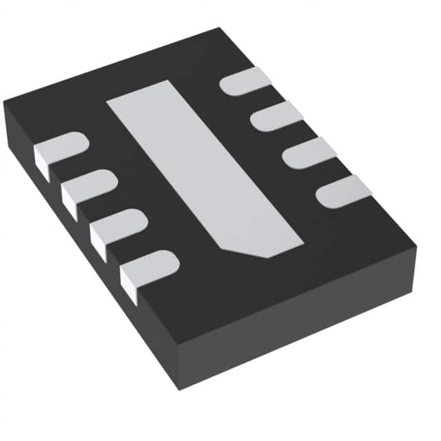
- Part No.:
- LTC4366CDDB-1#TRMPBF
- Manufacturer:
- Analog Devices Inc.
- Category:
- Surge Suppression Ics
- Package:
- 8-WFDFN Exposed Pad
- Datasheet:
-
 LTC4366CDDB-1#TRMPBF.pdf
- Description:
- IC SURGE STOPPER HV 8-DFN
- Quantity:
- Payment:

- Shipping:

Inventory:2,604
Please send an inquiry. Send us your inquiry, and we will respond immediately.
Product details
Overview
LTC4366CDDB-1#TRMPBF from Analog Devices is a high-voltage surge stopper IC that protects downstream loads by regulating output voltage during overvoltage transients using an external N-channel MOSFET. It features adjustable overvoltage clamping (via FB divider), 9-second internal cool-down timer, latch-off fault behavior (–1 version), and operates across 9V to >500V input range. It is used in 28V vehicle systems requiring uninterrupted operation under transient surges.
For engineers reviewing the LTC4366CDDB-1#TRMPBF datasheet, LTC4366CDDB-1#TRMPBF pinout, LTC4366CDDB-1#TRMPBF application, or LTC4366CDDB-1#TRMPBF equivalent, key selection criteria include its latched-off fault response, floating topology support, 0°C to 70°C temperature grade, DFN-8 (3mm × 2mm) package, and compatibility with high-voltage DC distribution architectures.
Technical Context
The LTC4366CDDB-1#TRMPBF implements a floating architecture where regulation circuitry is powered from the MOSFET source (OUT pin), enabling operation up to the MOSFET's breakdown voltage - not limited by IC pin ratings. Its overvoltage regulation amplifier maintains FB = OUT – 1.23V, controlling gate drive to clamp output at user-defined voltage via RFB1/RFB2.
It uses dual shunt regulators (VDD clamped at 11.7V typ, OUT clamped at 5.5V typ) and a charge pump (2MHz) to drive GATE 12V above OUT. The TIMER pin enables programmable overvoltage duration (default 1µs; capacitor sets 311ms/µF), after which it triggers a 9-second cool-down before latching off (LTC4366-1 variant).
Key Specifications
| Parameter | Value and Actual Design Meaning |
|---|---|
| Overvoltage Response | Regulates output at user-set voltage (e.g., 43V) during transient; drops excess voltage across external MOSFET while load remains powered. |
| Fault Behavior | LTC4366-1 variant latches off after overvoltage timeout; requires SD pin toggle to reset - prevents uncontrolled re-engagement. |
| Operating Voltage Range | Supports input supply from 9V to >500V via floating topology - VDD and OUT pins internally shunt-regulated (11.7V and 5.5V typical). |
| Package & Temp Grade | 8-lead (3mm × 2mm) plastic DFN; commercial grade (0°C to 70°C ambient) - validated for industrial and 28V vehicle system deployment. |
| Shutdown Quiescent Current | Reduces total IVDD + IOUT to <20µA when SD pulled >1.5V below VDD - enables low-power standby in battery-backed systems. |
| GATE Drive Capability | Drives external N-MOSFET gate up to 12V above OUT; includes fast discharge (200mA sink) and charge pump (20µA source) for full enhancement. |
| Protection Timers | Adjustable overvoltage timer (via TIMER pin capacitor); fixed 9-second cool-down period ensures MOSFET thermal recovery before reset attempt. |
Pinout & Package
Package: 8-lead (3mm × 2mm) plastic DFN (DDB), exposed pad (optional VSS connection), θJA = 75°C/W when VSS soldered to PCB.
| Pin/Terminal | Circuit Role | Design Meaning |
|---|---|---|
| VDD | Start-up supply input | Provides 7.5µA gate-charge current during boot; clamped at 11.7V - powers logic and timer when MOSFET is off. |
| SD | Shutdown control input | Active-low enable: pulled up internally (1.6µA); requires >700µs low pulse >1.5V below VDD to enter <20µA shutdown state. |
| TIMER | Overvoltage duration setting | Charged at 9µA; fault triggered when voltage reaches 2.8V - capacitor value sets regulation window (311ms/µF). |
| VSS | Device return and substrate | Reference for all voltages; bypass capacitors for OUT and TIMER must connect here; exposed pad may be tied to VSS. |
| BASE | PNP base driver output | Connects to external PNP emitter (collector grounded) to reduce RSS power dissipation in high-voltage applications. |
| FB | Overvoltage feedback input | Senses voltage drop across RFB1; regulation amplifier holds FB = OUT – 1.23V - sets output clamp voltage via resistor divider. |
| OUT | Charge pump & regulation supply | Powered from MOSFET source; enables floating operation; clamped at 5.5V; supplies regulation amp and charge pump. |
| GATE | N-MOSFET gate driver output | Drives external MOSFET gate; includes 200mA fast-discharge path during overvoltage; clamped 12V above OUT. |
Key Features
| Feature | Design Value |
|---|---|
| Floating topology support | Enables >500V input protection by powering regulation circuitry from MOSFET source (OUT), isolating IC from input surge. |
| Adjustable overvoltage clamp | Output regulated at precise voltage (e.g., 43V) via external RFB1/RFB2 divider - no internal reference dependency on supply rail. |
| Latched-off fault response | LTC4366-1 variant remains disabled after overvoltage timeout until SD pin is actively toggled - prevents unsafe auto-restart. |
| Thermally managed protection | 9-second cool-down timer ensures MOSFET junction temperature recovers before reset - avoids cumulative thermal stress. |
| Low-quiescent shutdown | Reduces combined IVDD + IOUT to <20µA in shutdown - preserves battery life in always-on vehicle or avionic systems. |
Applications
| 28V Vehicle Power Distribution | Avionic High-Voltage DC Bus |
|---|---|
Use Scenario: Protecting flight control electronics from 250V transients on MIL-STD-704-compliant 28V aircraft bus. IC Role / Device Role / Timing Role: Surge stopper regulating output at 43V while maintaining uninterrupted power to critical loads. Use Value: Prevents MOSFET destruction during lightning-induced surges; latched-off behavior avoids uncontrolled restart during fault persistence. |
Use Scenario: Safeguarding navigation computers against load-dump spikes in airborne power systems with >400V transient capability. IC Role / Device Role / Timing Role: Floating overvoltage protector controlling external N-MOSFET gate to clamp output during EMI-coupled transients. Use Value: Enables use of cost-effective 600V MOSFETs without derating; DFN-8 package supports compact, high-density avionic board layouts. |
| Industrial High-Voltage DC Links | Rugged Floating Power Supplies |
Use Scenario: Securing PLC I/O modules connected to 300V DC distribution rails in factory automation systems. IC Role / Device Role / Timing Role: Overvoltage regulator with programmable timer limiting MOSFET conduction time during sustained overvoltage events. Use Value: Eliminates need for bulky TVS diodes; 9-second cool-down prevents thermal runaway in enclosed enclosures. |
Use Scenario: Building isolated, wide-input-range power supplies for test equipment operating from 12V to 500V sources. IC Role / Device Role / Timing Role: Core surge management IC enabling floating topology with external PNP-assisted RSS current reduction. Use Value: Reduces physical size of voltage-dropping resistors by 35× using BASE-driven PNP - critical for portable instrumentation. |
Equivalent & Alternatives
The following parts are listed as comparable options for similar overvoltage protection applications.
| Alternative Part | Technical Difference | Application Difference | Selection Advice |
|---|---|---|---|
| LTC4366IDDB-1#TRMPBF | Same functionality and pinout; extended temperature range (–40°C to 85°C) vs. LTC4366CDDB-1#TRMPBF's 0°C to 70°C. | Required for automotive under-hood or industrial outdoor deployments where ambient exceeds 70°C. | Select when operating environment exceeds commercial temperature limits; otherwise LTC4366CDDB-1#TRMPBF is optimal for cost-sensitive 28V vehicle cabin systems. |
| LTC4366CDDB-2#TRMPBF | Identical package and specs except auto-retry fault behavior (9-second cool-down then automatic restart) vs. latch-off of LTC4366CDDB-1#TRMPBF. | Suitable for non-critical loads where brief interruption is acceptable; unsuitable for safety-critical systems requiring manual fault acknowledgment. | Choose LTC4366CDDB-2#TRMPBF only if system-level fault handling permits autonomous recovery; LTC4366CDDB-1#TRMPBF is preferred for deterministic, operator-controlled reset. |
Compared with LTC4366IDDB-1#TRMPBF, the LTC4366CDDB-1#TRMPBF offers lower cost and smaller thermal footprint in commercial-temperature applications; versus LTC4366CDDB-2#TRMPBF, it provides fail-safe latched behavior essential for mission-critical power domains where unattended restart is prohibited.
Availability
LTC4366CDDB-1#TRMPBF is available at Aetrix Electronics and suitable for 28V vehicle systems, avionic DC distribution, and industrial high-voltage power supplies requiring stable component supply, long-term lifecycle assurance, and RoHS-compliant packaging.
Supply support for LTC4366CDDB-1#TRMPBF includes scheduled delivery planning, volume procurement assistance, BOM continuity management, traceable sourcing, and lifecycle availability coordination for OEM customers, industrial embedded developers, connected-device designers, and electronics production programs.
Manufacturer
Analog Devices (now part of Analog Devices, Inc., a wholly owned subsidiary of Analog Devices, Inc.) designs precision analog, mixed-signal, and digital signal processing ICs for high-reliability applications.
The LTC4366 product line delivers high-voltage surge protection ICs optimized for floating topologies in aerospace, automotive, and industrial power systems - enabling robust overvoltage resilience without compromising load uptime.
FAQ
What is the fault response behavior of the LTC4366CDDB-1#TRMPBF?
The LTC4366CDDB-1#TRMPBF implements a latched-off fault response: upon overvoltage timeout, it disables the external MOSFET and remains off until the SD pin is actively toggled low then high. This prevents uncontrolled re-engagement during persistent overvoltage conditions and is distinct from the auto-retry behavior of the LTC4366CDDB-2#TRMPBF variant. The latch ensures deterministic system-level fault handling in safety-critical applications.
How does the LTC4366CDDB-1#TRMPBF achieve >500V input capability despite its 12V-rated pins?
The LTC4366CDDB-1#TRMPBF achieves >500V input capability through a floating architecture: its regulation circuitry is powered from the MOSFET source (OUT pin), not the input rail. VDD and OUT pins are internally shunt-regulated (11.7V and 5.5V typical), isolating sensitive circuitry from input transients. The external MOSFET bears the full surge voltage, while the LTC4366CDDB-1#TRMPBF only sees clamped, safe internal rails - enabling protection far beyond its pin voltage ratings.
What is the role of the BASE pin on the LTC4366CDDB-1#TRMPBF?
The BASE pin on the LTC4366CDDB-1#TRMPBF drives the base of an external PNP transistor to reduce power dissipation in the RSS resistor. By sourcing ~0.8µA plus PNP base current, it allows RSS values up to 35× larger than in standard configurations - significantly shrinking resistor size and thermal footprint in high-voltage applications like avionic DC buses. When unused, BASE must be tied to VSS.
Can the LTC4366CDDB-1#TRMPBF regulate output voltage at precisely 43V?
Yes - the LTC4366CDDB-1#TRMPBF regulates output voltage at precisely 43V (or any user-defined level) using the FB pin feedback network. The overvoltage regulation amplifier holds FB = OUT – 1.23V; selecting RFB1 = 12.4kΩ and RFB2 = 422kΩ (as shown in the典型 application) sets VOUT = 1.23V × (1 + RFB2/RFB1) ≈ 43V. This ratio-based clamping is stable across temperature and supply variations.
What is the purpose of the TIMER pin on the LTC4366CDDB-1#TRMPBF?
The TIMER pin on the LTC4366CDDB-1#TRMPBF controls overvoltage regulation duration: during clamping, it charges at 9µA until reaching 2.8V, triggering fault shutdown. With no capacitor, regulation lasts ~1µs; adding CT = 8.2nF extends it to ~25.5ms (311ms/µF rule). This prevents MOSFET thermal damage during sustained overvoltage - a critical safeguard absent in basic crowbar solutions.
LTC4366CDDB-1#TRMPBF Specifications
- Product attributes
- Attribute value
- Manufacturer:
- Analog Devices Inc.
- Package/Case:
- 8-WFDFN Exposed Pad
- Series:
- -
- Packaging:
- Tape & Reel (TR)
- Product Status:
- Active
- Voltage - Clamping:
- Adjustable
- Technology:
- External Switch
- Number of Circuits:
- 1
- Applications:
- -
- Grade:
- Automotive
- Qualification:
- -
- Mounting Type:
- Surface Mount
- Supplier Device Package:
- 8-DFN (3x2)
LTC4366CDDB-1#TRMPBF FAQ
1.How can I place an order for LTC4366CDDB-1#TRMPBF through Aetrix?
Please submit a Request for Quotation (RFQ) for LTC4366CDDB-1#TRMPBF on Aetrix. Our sales agent will provide a competitive quotation and guide you through the order confirmation once you accept the terms.
2.Are the price and stock information for LTC4366CDDB-1#TRMPBF reliable?
The price and inventory of LTC4366CDDB-1#TRMPBF are updated periodically and may fluctuate due to market conditions. Stock and pricing data are typically refreshed every 24 hours. Quotation validity for LTC4366CDDB-1#TRMPBF is usually 5 days.
3.What payment methods are accepted for LTC4366CDDB-1#TRMPBF?
We accept Wire Transfer, PayPal, Credit Card, Western Union, MoneyGram, and Escrow for LTC4366CDDB-1#TRMPBF transactions.
Note: Certain payment methods may incur a processing fee.
4.How is shipping managed for LTC4366CDDB-1#TRMPBF?
LTC4366CDDB-1#TRMPBF orders can be shipped via leading logistics carriers, including DHL, UPS, FedEx, TNT, or Registered Mail.
Once your LTC4366CDDB-1#TRMPBF order is processed, you will receive an email with the shipment details and tracking number.
Note: Tracking information may take up to 24 hours to appear. Express delivery typically takes 3–5 business days.
5.How can I obtain technical support or documentation for LTC4366CDDB-1#TRMPBF?
For technical support, including LTC4366CDDB-1#TRMPBF datasheets, pinout diagrams, or application guidance, please contact our engineering support team. They can provide detailed documentation and assistance for your LTC4366CDDB-1#TRMPBF requirements.
6.How does Aetrix verify that LTC4366CDDB-1#TRMPBF is sourced from the original manufacturer or authorized distributors?
All LTC4366CDDB-1#TRMPBF products on Aetrix are procured from qualified distributors and authorized channels. Our dedicated quality assurance team conducts strict verification, including traceability checks and, if necessary, third-party testing. This ensures that LTC4366CDDB-1#TRMPBF meets industry standards.
7.What is the process for return or replacement of LTC4366CDDB-1#TRMPBF?
All LTC4366CDDB-1#TRMPBF units undergo pre-shipment inspection (PSI). If there is an issue with LTC4366CDDB-1#TRMPBF, returns or replacements are accepted under the following conditions:
1.Quantity discrepancies, incorrect items, or visible external defects (such as breakage or corrosion), acknowledged by Aetrix.
2.The issue is reported within 90 days of delivery.
3.The LTC4366CDDB-1#TRMPBF part is unused and in its original packaging.
Return procedure for LTC4366CDDB-1#TRMPBF:
1.Submit a request within 90 days.
2.Obtain a Return Material Authorization (RMA) from Aetrix.
LTC4366CDDB-1#TRMPBF Tags
-
TVS3300DRVR
Texas Instruments

-
TCPP01-M12
STMicroelectronics
-
TPD4S214YFFR
Texas Instruments
-
TPD6S300ARUKR
Texas Instruments
-
TBU-CA085-300-WH
Bourns Inc.
-
TBU-CA065-500-WH
Bourns Inc.
-
TBU-CA040-100-WH
Bourns Inc.
-
TBU-CA085-500-WH
Bourns Inc.
-
TBU-CA085-200-WH
Bourns Inc.
-
NX20P0408UKZ
NXP Semiconductors
-
TBU-CA085-100-WH
Bourns Inc.
-
TBU-CA050-300-WH
Bourns Inc.
Tech Hub

A practical engineering guide to 3.3V and 5V logic compatibility, input thresholds, resistor dividers, translator ICs, MOSFET level shifting, I2C pull-ups, timing limits and power-sequencing risks.

The 74HC595 uses push-pull logic outputs, while the TPIC6B595 uses 50 V open-drain DMOS sinks for higher-power loads. This guide compares timing, current limits, 3.3 V interfacing, load wiring, thermal…

The 74HC595 converts serial data into eight stable parallel outputs. This guide covers pin functions, shift and storage timing, OE and MR behavior, drive-current limits, cascading, voltage compatibilit…

A technical comparison of level-sensitive latches and edge-triggered flip-flops, covering timing windows, setup and hold limits, master–slave operation, time borrowing, race-through, HDL inference and…

A D latch stores one bit while Enable controls when data can pass. This reference covers gate-level operation, truth tables, transparency, setup and hold timing, LE versus OE, common ICs and practical …

An SR latch stores one bit through cross-coupled feedback. This engineering reference covers NOR and NAND implementations, truth tables, forbidden-state recovery, gated operation, switch debouncing, fa…

Latch circuits retain one bit through feedback. This technical reference covers SR and D latches, truth tables, transparency, timing limits, latch-versus-flip-flop behavior, applications and common log…

An engineering guide to LED driver operation, constant-current and constant-voltage outputs, linear and switching topologies, dimming, IC selection, calculations, replacement compatibility, and fault c…

Operational amplifier guide covering op amp basics, feedback, ideal vs real op amps, common configurations, buffer circuits, offset, bias current, gain-bandwidth, slew rate, rail-to-rail limits and sel…

Jumper cables guide covering safe connection order, red and black clamp placement, final ground connection, cable gauge, length, clamp quality, copper vs CCA cables, jump starter comparison and battery…


