
 My Inquiry
 My Account


Analog Devices Inc. LTC4367HMS8#PBF
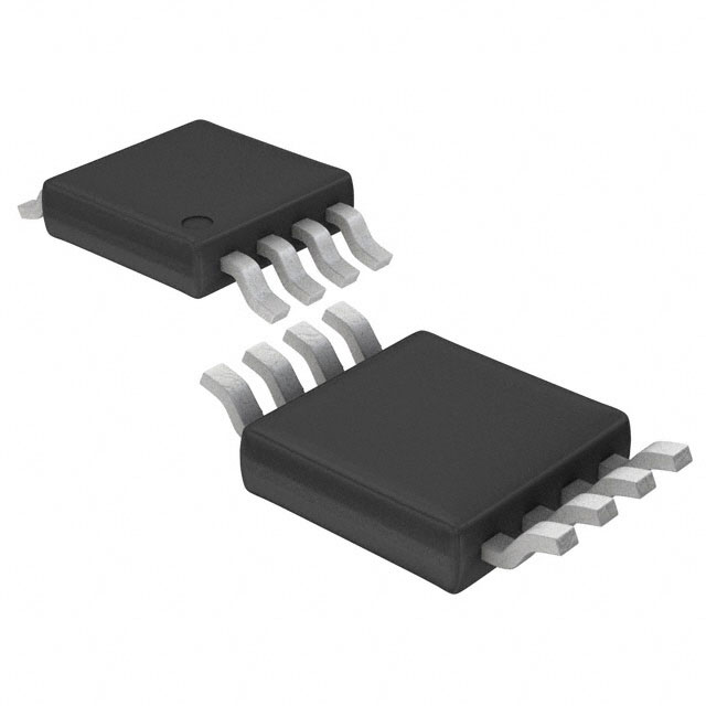
- Part No.:
- LTC4367HMS8#PBF
- Manufacturer:
- Analog Devices Inc.
- Category:
- Power Management - Specialized
- Package:
- 8-TSSOP, 8-MSOP (0.118", 3.00mm Width)
- Datasheet:
-
 LTC4367HMS8#PBF.pdf
- Description:
- SUPPLY PROTECTION CONTROLLER
- Quantity:
- Payment:

- Shipping:

Inventory:1,681
Please send an inquiry. Send us your inquiry, and we will respond immediately.
Product details
Overview
LTC4367HMS8#PBF from Analog Devices is a high-voltage overvoltage, undervoltage, and reverse supply protection controller that controls back-to-back N-channel MOSFETs to safeguard downstream loads. It operates from 2.5V to 60V, withstands –40V to 100V fault transients, features adjustable UV/OV thresholds (±25mV hysteresis), delivers 13.1V gate drive enhancement, and consumes only 70µA quiescent current - enabling robust automotive load-dump and industrial surge protection.
For engineers reviewing the LTC4367HMS8#PBF datasheet, LTC4367HMS8#PBF pinout, LTC4367HMS8#PBF application, or LTC4367HMS8#PBF equivalent, key selection criteria include its –40°C to 125°C operating temperature range, 32ms fault recovery delay, MSOP-8 package with exposed pad, and compatibility with dual N-channel MOSFETs such as Si7942 for 100V-rated systems.
Technical Context
The LTC4367HMS8#PBF integrates two precision comparators (0.5V threshold, 1µs propagation) for user-configurable UV and OV monitoring via external resistive dividers, coupled with a high-voltage charge pump that drives GATE up to 13.1V above VOUT. Its reverse protection circuitry actively clamps GATE to VIN during negative input events, ensuring M2 remains off while blocking –40V faults.
It implements a 32ms turn-on delay timer after fault clearance to suppress 50/60Hz AC coupling and line noise-induced chatter, and provides controlled shutdown via SHDN with 90µA gate pull-down and GATE-to-VOUT tracking during VOUT decay - critical for low-slew-rate inrush control in automotive and industrial power rails.
Key Specifications
| Parameter | Value and Actual Design Meaning |
|---|---|
| Operating Voltage Range | 2.5V to 60V - defines functional input supply window for normal system operation. |
| Protection Range | –40V to 100V - specifies absolute fault voltage limits the device survives without damage. |
| UV/OV Threshold Accuracy | ±7.5mV at 25°C (500mV nominal) - enables precise 3.5V–18V or similar custom window setting with <1% resistor networks. |
| Gate Drive Enhancement | Up to 13.1V above VOUT - ensures full enhancement of standard N-channel MOSFETs (e.g., Si7942) even at low VIN. |
| Quiescent Current | 70µA typical - allows always-on protection in battery-backed or low-power industrial systems. |
| Shutdown Current | 5µA maximum - supports ultra-low standby power during system sleep or disable states. |
| Turn-On Delay (tD(ON)) | 32ms typical - filters 50/60Hz AC interference and prevents false re-engagement after transient overvoltage. |
Pinout & Package
Package: 8-Lead Plastic MSOP (MS8) with exposed pad (optional ground connection). Dimensions: 3mm × 3mm footprint, 1.1mm height. Thermal resistance θJA = 160°C/W.
| Pin/Terminal | Circuit Role | Design Meaning |
|---|---|---|
| VIN | High-voltage input supply rail | Accepts –40V to 100V; powers internal LDO and serves as primary fault sensing node. |
| UV | Undervoltage comparator input | Monitors VIN via resistive divider; triggers fault if voltage falls below user-set threshold (e.g., 3.5V). |
| OV | Overvoltage comparator input | Monitors VIN via resistive divider; asserts fault if voltage exceeds user-set threshold (e.g., 18V). |
| GND | Device ground reference | Common return for internal circuitry and external feedback paths; connects to PCB ground plane. |
| GATE | Gate drive output | Drives gates of external back-to-back N-MOSFETs; referenced to VOUT; pulls down to ~VOUT during fault. |
| VOUT | Output voltage sense input | Senses load-side voltage; used as charge pump reference and enables accurate gate drive regulation. |
| FAULT | Open-drain fault indicator | Pulled low during UV/OV fault, SHDN assertion, or VIN < UVLO; sinks up to 500µA for external logic interfacing. |
| SHDN | Shutdown control input | Active-low enable; places device in 5µA shutdown mode and initiates controlled gate discharge. |
Key Features
| Feature | Design Value |
|---|---|
| No input capacitor or TVS required | Enables compact, cost-optimized designs by eliminating external surge suppression components for most 100V-class transients. |
| Reverse supply protection to –40V | Automatically disconnects load when VIN is reversed or negative, using internal switch to clamp GATE to VIN. |
| Adjustable UV/OV thresholds | Allows precise customization of safe operating window (e.g., 7V–36V) using standard 1% resistors without trimming. |
| Low 70µA operating current | Supports continuous protection in energy-sensitive applications like portable instrumentation and remote sensors. |
| 32ms fault recovery delay | Prevents oscillation during noisy or marginal supply conditions, including AC line coupling and load-dump ringing. |
Applications
| Automotive Load-Dump Protection | Industrial Power Input Conditioning |
|---|---|
Use Scenario: Protecting ECUs and infotainment modules from ISO 7637-2 Pulse 5a/b load-dump transients up to +100V. IC Role / Device Role / Timing Role: Acts as front-end protection controller, isolating downstream DC/DC converters and microcontrollers from faulted battery rails. Use Value: Eliminates need for high-voltage TVS diodes and series P-MOSFETs, reducing BOM count and board area while maintaining –40°C to 125°C operation. | Use Scenario: Securing programmable logic controllers (PLCs) and I/O modules against field-wiring errors and AC-coupled surges in factory automation. IC Role / Device Role / Timing Role: Provides programmable UV lockout (e.g., 18V min) and OV cutoff (e.g., 36V max) before power reaches sensitive FPGA or ADC subsystems. Use Value: Enables single-rail 24V system design with guaranteed fault isolation, avoiding costly redesigns due to miswired 48V supplies or reversed polarity connections. |
| Portable Instrumentation Power Management | Network Equipment DC Input Protection |
Use Scenario: Safeguarding handheld test equipment powered by interchangeable AC adapters or Li-ion batteries with variable polarity. IC Role / Device Role / Timing Role: Serves as polarity-agnostic input supervisor, blocking reverse battery insertion and overvoltage AC adapter mismatches. Use Value: Prevents catastrophic damage from user-induced faults while consuming only 70µA - extending battery life in always-on measurement devices. | Use Scenario: Protecting PoE-powered switches and base station radios from DC input faults caused by faulty power injectors or lightning-induced surges. IC Role / Device Role / Timing Role: Functions as primary DC input guard, rejecting –40V reverse bias and +100V transients before they reach isolated DC/DC stages. Use Value: Achieves IEC 61000-4-5 Level 4 surge immunity without external crowbar circuits, simplifying compliance testing and certification. |
Equivalent & Alternatives
The following parts are listed as comparable options for similar overvoltage/undervoltage protection applications.
| Alternative Part | Technical Difference | Application Difference | Selection Advice |
|---|---|---|---|
| LTC4367HDD#PBF | Same functionality and specs, but in 3mm × 3mm DFN-8 package with θJA = 43°C/W - superior thermal performance. | Better suited for high-power density layouts or thermally constrained enclosures where MSOP footprint is insufficient. | Select LTC4367HDD#PBF when PCB space allows DFN placement and thermal management is prioritized over legacy MSOP compatibility. |
| LTC4367HMS8-1#PBF | Identical pinout and package, but with 500µs GATE turn-on delay instead of 32ms - optimized for fast-recovery systems. | Required where rapid re-engagement after brief transients is critical (e.g., real-time control loops), not for AC-line rejection. | Choose LTC4367HMS8-1#PBF only when 500µs recovery is explicitly needed; otherwise LTC4367HMS8#PBF's 32ms delay provides superior noise immunity. |
Compared with LTC4367HDD#PBF, the LTC4367HMS8#PBF offers identical electrical behavior but higher thermal resistance (160°C/W vs 43°C/W), making it suitable for lower-power deployments or legacy MSOP-based designs; versus LTC4367HMS8-1#PBF, it trades faster recovery for stronger 50/60Hz AC blocking and transient noise rejection.
Availability
LTC4367HMS8#PBF is available at Aetrix Electronics and suitable for automotive ECU protection, industrial PLC input conditioning, and portable instrumentation requiring stable component supply across extended temperature ranges.
Supply support for LTC4367HMS8#PBF includes scheduled delivery planning, volume procurement assistance, BOM continuity management, traceable sourcing, and lifecycle availability coordination for OEM customers, industrial embedded developers, connected-device designers, and electronics production programs.
Manufacturer
Analog Devices (acquired Linear Technology in 2017) is a global leader in high-performance analog, mixed-signal, and power management ICs, serving precision instrumentation, industrial, automotive, and communications markets.
The LTC4367 product line delivers rugged, high-voltage input protection controllers designed specifically for automotive load-dump resilience, industrial field-wiring fault tolerance, and portable equipment polarity-agnostic power management.
FAQ
What is the maximum fault voltage the LTC4367HMS8#PBF can withstand without damage?
The LTC4367HMS8#PBF has an absolute maximum rating of –40V to 100V on the VIN pin. This means it can survive reverse polarity connections down to –40V and overvoltage transients up to +100V without permanent damage, though normal operation remains limited to 2.5V–60V. The device uses internal clamping and reverse-protection circuitry to isolate the load under these extreme conditions, making it ideal for automotive and industrial environments where such faults occur.
How does the LTC4367HMS8#PBF implement reverse supply protection?
The LTC4367HMS8#PBF detects negative VIN via an internal comparator and immediately connects the GATE pin to VIN through an internal switch. This forces the gate of the downstream N-channel MOSFET (M2) to track the negative input, keeping it fully off while its body diode blocks reverse current flow. Unlike passive diode solutions, this active method achieves near-zero forward voltage drop during normal operation and full –40V blocking without external components - a key advantage over traditional P-MOSFET or Schottky approaches.
What is the purpose of the 32ms turn-on delay in the LTC4367HMS8#PBF?
The 32ms turn-on delay (tD(ON)) in the LTC4367HMS8#PBF acts as a debouncing filter after UV or OV faults clear, preventing chattering caused by line noise, 50/60Hz AC coupling, or marginal supply recovery. It ensures the input remains stably within the user-defined UV/OV window for at least 32ms before re-enabling the external MOSFETs. This timing is fixed for the LTC4367HMS8#PBF variant and distinguishes it from the -1 version, which uses 500µs for fast-recovery applications.
Can the LTC4367HMS8#PBF be used with standard N-channel MOSFETs like Si7942?
Yes, the LTC4367HMS8#PBF is explicitly validated with dual N-channel MOSFETs such as the Si7942 (100V, 49mΩ). Its gate drive delivers up to 13.1V enhancement above VOUT, sufficient to fully enhance standard logic-level or standard-threshold N-MOSFETs across the full 2.5V–60V operating range. The datasheet provides resistor selection guidelines and MOSFET compatibility tables confirming Si7942 usage in 24V automotive and 48V industrial configurations with the LTC4367HMS8#PBF.
What is the operating temperature range of the LTC4367HMS8#PBF?
The LTC4367HMS8#PBF is rated for operation from –40°C to +125°C ambient temperature, qualifying it for under-hood automotive, industrial control cabinet, and outdoor telecom applications. This H-grade specification matches the extended temperature performance of its internal comparators, charge pump, and fault timers - all characterized across the full range - unlike commercial-grade variants (C-grade: 0°C–70°C or I-grade: –40°C–85°C).
LTC4367HMS8#PBF Specifications
- Product attributes
- Attribute value
- Manufacturer:
- Analog Devices Inc.
- Series:
- -
- Package/Case:
- 8-TSSOP, 8-MSOP (0.118", 3.00mm Width)
- Packaging:
- Tube
- Product Status:
- Active
- Applications:
- Overvoltage, Undervoltage Protection
- Current - Supply:
- 70µA
- Voltage - Supply:
- 2.5V ~ 60V
- Operating Temperature:
- -40°C ~ 125°C
- Grade:
- -
- Qualification:
- -
- Mounting Type:
- Surface Mount
- Supplier Device Package:
- 8-MSOP
LTC4367HMS8#PBF FAQ
1.How can I place an order for LTC4367HMS8#PBF through Aetrix?
Please submit a Request for Quotation (RFQ) for LTC4367HMS8#PBF on Aetrix. Our sales agent will provide a competitive quotation and guide you through the order confirmation once you accept the terms.
2.Are the price and stock information for LTC4367HMS8#PBF reliable?
The price and inventory of LTC4367HMS8#PBF are updated periodically and may fluctuate due to market conditions. Stock and pricing data are typically refreshed every 24 hours. Quotation validity for LTC4367HMS8#PBF is usually 5 days.
3.What payment methods are accepted for LTC4367HMS8#PBF?
We accept Wire Transfer, PayPal, Credit Card, Western Union, MoneyGram, and Escrow for LTC4367HMS8#PBF transactions.
Note: Certain payment methods may incur a processing fee.
4.How is shipping managed for LTC4367HMS8#PBF?
LTC4367HMS8#PBF orders can be shipped via leading logistics carriers, including DHL, UPS, FedEx, TNT, or Registered Mail.
Once your LTC4367HMS8#PBF order is processed, you will receive an email with the shipment details and tracking number.
Note: Tracking information may take up to 24 hours to appear. Express delivery typically takes 3–5 business days.
5.How can I obtain technical support or documentation for LTC4367HMS8#PBF?
For technical support, including LTC4367HMS8#PBF datasheets, pinout diagrams, or application guidance, please contact our engineering support team. They can provide detailed documentation and assistance for your LTC4367HMS8#PBF requirements.
6.How does Aetrix verify that LTC4367HMS8#PBF is sourced from the original manufacturer or authorized distributors?
All LTC4367HMS8#PBF products on Aetrix are procured from qualified distributors and authorized channels. Our dedicated quality assurance team conducts strict verification, including traceability checks and, if necessary, third-party testing. This ensures that LTC4367HMS8#PBF meets industry standards.
7.What is the process for return or replacement of LTC4367HMS8#PBF?
All LTC4367HMS8#PBF units undergo pre-shipment inspection (PSI). If there is an issue with LTC4367HMS8#PBF, returns or replacements are accepted under the following conditions:
1.Quantity discrepancies, incorrect items, or visible external defects (such as breakage or corrosion), acknowledged by Aetrix.
2.The issue is reported within 90 days of delivery.
3.The LTC4367HMS8#PBF part is unused and in its original packaging.
Return procedure for LTC4367HMS8#PBF:
1.Submit a request within 90 days.
2.Obtain a Return Material Authorization (RMA) from Aetrix.
LTC4367HMS8#PBF Tags

-
TPS2511DGNR
Texas Instruments

-
UTC2000/MG
Microchip Technology

-
TUSB320HAIRWBR
Texas Instruments

-
TPS61252DSGR
Texas Instruments

-
PI5USB30216CXUAEX
Diodes Incorporated

-
SN6501DBVR
Texas Instruments

-
CYPD3177-24LQXQT
Infineon Technologies
-
SN6501QDBVRQ1
Texas Instruments

-
STUSB1600AQTR
STMicroelectronics

-
SN6505BDBVR
Texas Instruments
-
SN6501DBVT
Texas Instruments

-
TPS65150PWPR
Texas Instruments
Tech Hub

A practical engineering guide to 3.3V and 5V logic compatibility, input thresholds, resistor dividers, translator ICs, MOSFET level shifting, I2C pull-ups, timing limits and power-sequencing risks.

The 74HC595 uses push-pull logic outputs, while the TPIC6B595 uses 50 V open-drain DMOS sinks for higher-power loads. This guide compares timing, current limits, 3.3 V interfacing, load wiring, thermal…

The 74HC595 converts serial data into eight stable parallel outputs. This guide covers pin functions, shift and storage timing, OE and MR behavior, drive-current limits, cascading, voltage compatibilit…

A technical comparison of level-sensitive latches and edge-triggered flip-flops, covering timing windows, setup and hold limits, master–slave operation, time borrowing, race-through, HDL inference and…

A D latch stores one bit while Enable controls when data can pass. This reference covers gate-level operation, truth tables, transparency, setup and hold timing, LE versus OE, common ICs and practical …

An SR latch stores one bit through cross-coupled feedback. This engineering reference covers NOR and NAND implementations, truth tables, forbidden-state recovery, gated operation, switch debouncing, fa…

Latch circuits retain one bit through feedback. This technical reference covers SR and D latches, truth tables, transparency, timing limits, latch-versus-flip-flop behavior, applications and common log…

An engineering guide to LED driver operation, constant-current and constant-voltage outputs, linear and switching topologies, dimming, IC selection, calculations, replacement compatibility, and fault c…

Operational amplifier guide covering op amp basics, feedback, ideal vs real op amps, common configurations, buffer circuits, offset, bias current, gain-bandwidth, slew rate, rail-to-rail limits and sel…

Jumper cables guide covering safe connection order, red and black clamp placement, final ground connection, cable gauge, length, clamp quality, copper vs CCA cables, jump starter comparison and battery…


