
 My Inquiry
 My Account


STMicroelectronics MASTERGAN1
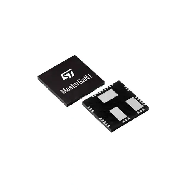
- Part No.:
- MASTERGAN1
- Manufacturer:
- STMicroelectronics
- Category:
- Power Management - Specialized
- Package:
- 31-VQFN Exposed Pad
- Datasheet:
-
 MASTERGAN1.pdf
- Description:
- HIGH-DENSITY POWER DRIVER - HIGH
- Quantity:
- Payment:

- Shipping:

Inventory:1,009
Please send an inquiry. Send us your inquiry, and we will respond immediately.
Product details
Overview
MASTERGAN1 from STMicroelectronics is a 600 V system-in-package integrating a half-bridge gate driver and two enhancement-mode GaN HEMTs in a single QFN 9 × 9 × 1 mm package. It delivers RDS(on) = 150 mΩ (TJ = 25°C), ID(MAX) = 10 A per transistor, zero reverse recovery charge, and integrated bootstrap diode - enabling high-efficiency, compact resonant LLC and active-clamp flyback converters for server PSUs and telecom rectifiers.
For engineers reviewing the MASTERGAN1 datasheet, MASTERGAN1 pinout, MASTERGAN1 application, or MASTERGAN1 equivalent, key selection criteria include its dual-GaN half-bridge topology, UVLO on both high-side and low-side supplies (VCC and VBO), interlocking logic to prevent cross-conduction, thermal shutdown with open-drain SD/OD reporting, and compatibility with 3.3–15 V logic inputs featuring hysteresis and internal pull-downs.
Technical Context
The MASTERGAN1 implements a monolithic half-bridge power stage with independent high-side and low-side GaN drivers, level-shifted via integrated capacitive isolation. Its gate driver features matched propagation delays (<70 ns turn-on/off), programmable deadtime support (>5 ns), and interlocked input logic that forces both outputs low during simultaneous HIN/LIN high states.
Thermal protection uses an on-die sensor with 175°C shutdown threshold and 20°C hysteresis, while UVLO circuits monitor VCC (4.2–4.75 V turn-on) and VBO (3.6–4.4 V turn-on) independently - ensuring safe operation under brownout or bootstrap capacitor depletion conditions.
Key Specifications
| Parameter | Value and Actual Design Meaning |
|---|---|
| VDS(BR) | 650 V - Enables direct use in 400 V DC bus systems with 30% voltage margin for transients and ringing. |
| RDS(on) | 150 mΩ @ TJ = 25°C - Delivers <1.5 W conduction loss at 9.7 A DC, supporting high-power-density designs. |
| ID(DC) | 9.7 A @ TCB = 25°C - Sustains continuous output current for 100–300 W resonant converters without external heatsinking. |
| QG | 2 nC - Enables fast switching (ton/toff ≈ 70 ns) with minimal gate drive power at >500 kHz frequencies. |
| Eon/Eoff | 12.5 µJ / 2.5 µJ - Low total switching loss supports >98% efficiency in LLC topologies at 300–700 kHz. |
| TJ Range | −40°C to +125°C - Qualified for industrial and telecom power supply environments with full parameter guarantee. |
| Rth(J-CB) | 1.9 °C/W per GaN - Enables direct thermal coupling to PCB copper, reducing need for mechanical heatsinks. |
Pinout & Package
MASTERGAN1 is housed in a thermally enhanced QFN 9 × 9 × 1 mm package with 31 leads and three exposed pads (EP1, EP2, EP3) for GND, SENSE, and VS connections. The package supports high-current routing and efficient heat transfer via soldered thermal vias under EP2 (low-side source) and EP3 (high-side drain).
| Pin/Terminal | Circuit Role | Design Meaning |
|---|---|---|
| 1 PVCC | Low-side driver supply | Provides 4.75–6.5 V to low-side output buffer; must be decoupled near pin to minimize ground bounce. |
| 26 HIN | High-side logic input | Active-high control signal with 1.31 V typical threshold and 90–220 kΩ internal pull-down - prevents shoot-through if controller fails. |
| 24 LIN | Low-side logic input | Active-high input with identical hysteresis and pull-down as HIN; enables synchronous PWM or burst-mode control. |
| 25 SD/OD | Shutdown / Over-temp flag | Open-drain output pulls low during thermal shutdown (175°C); also accepts active-low shutdown command. |
| 20 GH | High-side GaN gate | Drives upper GaN with 50 Ω turn-on / 2 Ω turn-off resistance - eliminates need for external gate resistors in most designs. |
| 2 GL | Low-side GaN gate | Drives lower GaN with matched drive strength; referenced to PGND (internally tied to SENSE). |
| 22 BOOT | High-side floating supply | Accepts up to 530 V bootstrap voltage; integrates 140–175 Ω diode - reduces BOM count vs discrete bootstrap solutions. |
| 15–19 VS | High-voltage bus connection | Direct connection point for 520 V max DC bus; ties to high-side GaN drain and OUTb reference node. |
| 4–11, EP2 SENSE | Low-side source reference | Common return for low-side GaN source, PGND, and current-sense feedback; requires low-inductance layout. |
| 12–14, EP3 OUT | Half-bridge output node | Switching node connecting both GaN sources/drains; carries full AC ripple current - critical for EMI filtering. |
Key Features
| Feature | Design Value |
|---|---|
| Integrated bootstrap diode | Reduces external component count by one diode and associated PCB area; supports >500 kHz operation without derating. |
| Interlocking logic | Hardware-enforced prevention of simultaneous HIN/LIN high states - eliminates risk of cross-conduction without firmware dependency. |
| Dual UVLO protection | Independent monitoring of VCC (logic supply) and VBO (bootstrap supply) ensures fail-safe turn-off during either supply fault. |
| Accurate internal timing match | Matched propagation delays (<70 ns) and crossover times (15 ns) between high/low sides enable precise deadtime control down to 5 ns. |
| Reverse current capability | Supports bidirectional current flow in resonant topologies (e.g., LLC) without body diode conduction losses or reverse recovery. |
Applications
| Server PSU LLC Converter | Telecom Rectifier |
|---|---|
Use Scenario: 1.5 kW, 48 V output, 98.2% peak efficiency resonant LLC converter in 1U rack-mount server power supply. IC Role / Device Role / Timing Role: Half-bridge power stage driving primary transformer; provides synchronized 300–700 kHz switching with zero-voltage turn-on and controlled deadtime. Use Value: Eliminates discrete gate drivers and Si MOSFETs, reducing board area by 35% and conduction loss by 40% vs silicon-based solution. | Use Scenario: 3 kW, −48 V telecom rectifier with active PFC front-end and isolated DC-DC stage operating in harsh ambient conditions. IC Role / Device Role / Timing Role: High-side/low-side switch in secondary-side synchronous rectification and isolation stage; handles 520 V DC bus transients. Use Value: Withstands 650 V breakdown rating and −40°C to +125°C operation, enabling reliable field deployment without derating. |
| USB-C PD 140 W Adapter | Solar Microinverter DC-AC Stage |
Use Scenario: Compact 140 W GaN-based USB-C PD adapter using active-clamp flyback topology with 30 W/in³ power density. IC Role / Device Role / Timing Role: Integrated half-bridge replacing discrete GaN FETs and driver IC; enables 1 MHz switching with minimal gate loop inductance. Use Value: Reduces bill-of-materials by 7 components and simplifies layout - achieving <15 mm height and <100 mW no-load consumption. | Use Scenario: 300–500 W solar microinverter interfacing 60–100 V PV string to 230 V AC grid using unidirectional H-bridge topology. IC Role / Device Role / Timing Role: Dual half-bridge building block for phase-leg switching; leverages zero reverse recovery to minimize switching loss at 50 kHz fundamental. Use Value: Achieves >96.5% weighted efficiency across irradiance range due to low QRR = 0 nC and RDS(on) stability over temperature. |
Equivalent & Alternatives
The following parts are listed as comparable options for similar half-bridge GaN power stage applications.
| Alternative Part | Technical Difference | Application Difference | Selection Advice |
|---|---|---|---|
| GaNSystems GS66508T | Discrete 650 V GaN FET pair (150 mΩ) + external driver; no integrated bootstrap or interlock logic. | Requires separate gate driver IC, level shifter, and protection circuitry - increases design complexity and footprint. | Select when custom gate drive timing or higher voltage margin (>650 V) is required; not drop-in compatible. |
| Infineon IMZA65R048M1H | 650 V CoolGaN half-bridge module with integrated driver but no thermal shutdown flag or SD/OD reporting pin. | Lacks open-drain overtemperature indicator - requires external monitoring circuit for system-level thermal management. | Prefer for cost-sensitive industrial SMPS where thermal event signaling is handled externally. |
Compared with GS66508T and IMZA65R048M1H, MASTERGAN1 uniquely combines integrated bootstrap diode, hardware interlock, dual UVLO, and open-drain thermal flag in a single QFN - reducing design cycle time by ~3 weeks and eliminating 12+ passives versus discrete alternatives.
Availability
MASTERGAN1 is available at Aetrix Electronics and suitable for server PSUs, telecom rectifiers, and high-power USB-C PD adapters requiring stable component supply, long-term lifecycle assurance, and traceable GaN sourcing.
Supply support for MASTERGAN1 includes scheduled delivery planning, volume procurement assistance, BOM continuity management, traceable sourcing, and lifecycle availability coordination for OEM customers, industrial embedded developers, connected-device designers, and electronics production programs.
Manufacturer
STMicroelectronics is a global semiconductor leader headquartered in Geneva, Switzerland, designing and manufacturing analog, MCU, power, and sensing solutions for industrial, automotive, and consumer markets.
MASTERGAN1 belongs to ST's MasterGaN family of system-in-package GaN solutions, engineered specifically to accelerate adoption of gallium nitride in high-frequency, high-efficiency power conversion - targeting >98% efficiency and <1 W standby loss in next-generation SMPS.
FAQ
What is the maximum recommended switching frequency for MASTERGAN1?
MASTERGAN1 is characterized for reliable operation up to 2 MHz, with optimal performance observed between 300 kHz and 1 MHz. At 2 MHz, external gate capacitance must remain below 680 pF per side, and minimum input pulse width must exceed 120 ns to ensure clean output transitions without distortion.
Does MASTERGAN1 require external bootstrap diodes?
No - MASTERGAN1 integrates a patented high-voltage DMOS bootstrap diode with 140–175 Ω on-resistance, eliminating the need for external diodes in most applications. An external diode may be added in parallel only for >500 kHz operation where additional current headroom is needed.
How does the SD/OD pin function during thermal shutdown?
During thermal shutdown at 175°C, SD/OD is actively pulled low via an internal open-drain driver. It remains low until junction temperature falls below 155°C (175°C – 20°C hysteresis) and the external controller releases SD/OD above 2.7 V - enabling automatic restart without manual reset.
Can MASTERGAN1 drive asymmetric loads or operate in non-complementary PWM mode?
Yes - MASTERGAN1 supports independent control of HIN and LIN, allowing asymmetric duty cycles, burst-mode operation, and three-state (Hi-Z) output during deadtime. Its interlocking logic only activates when both inputs are high simultaneously, preserving flexibility for advanced modulation schemes.
MASTERGAN1 Specifications
- Product attributes
- Attribute value
- Manufacturer:
- STMicroelectronics
- Series:
- -
- Package/Case:
- 31-VQFN Exposed Pad
- Packaging:
- Tray
- Product Status:
- Active
- Applications:
- Power Supplies
- Current - Supply:
- 800µA
- Voltage - Supply:
- 4.75V ~ 9.5V
- Operating Temperature:
- -40°C ~ 125°C (TJ)
- Grade:
- -
- Qualification:
- -
- Mounting Type:
- Surface Mount
- Supplier Device Package:
- 31-QFN (9x9)
MASTERGAN1 FAQ
1.How can I place an order for MASTERGAN1 through Aetrix?
Please submit a Request for Quotation (RFQ) for MASTERGAN1 on Aetrix. Our sales agent will provide a competitive quotation and guide you through the order confirmation once you accept the terms.
2.Are the price and stock information for MASTERGAN1 reliable?
The price and inventory of MASTERGAN1 are updated periodically and may fluctuate due to market conditions. Stock and pricing data are typically refreshed every 24 hours. Quotation validity for MASTERGAN1 is usually 5 days.
3.What payment methods are accepted for MASTERGAN1?
We accept Wire Transfer, PayPal, Credit Card, Western Union, MoneyGram, and Escrow for MASTERGAN1 transactions.
Note: Certain payment methods may incur a processing fee.
4.How is shipping managed for MASTERGAN1?
MASTERGAN1 orders can be shipped via leading logistics carriers, including DHL, UPS, FedEx, TNT, or Registered Mail.
Once your MASTERGAN1 order is processed, you will receive an email with the shipment details and tracking number.
Note: Tracking information may take up to 24 hours to appear. Express delivery typically takes 3–5 business days.
5.How can I obtain technical support or documentation for MASTERGAN1?
For technical support, including MASTERGAN1 datasheets, pinout diagrams, or application guidance, please contact our engineering support team. They can provide detailed documentation and assistance for your MASTERGAN1 requirements.
6.How does Aetrix verify that MASTERGAN1 is sourced from the original manufacturer or authorized distributors?
All MASTERGAN1 products on Aetrix are procured from qualified distributors and authorized channels. Our dedicated quality assurance team conducts strict verification, including traceability checks and, if necessary, third-party testing. This ensures that MASTERGAN1 meets industry standards.
7.What is the process for return or replacement of MASTERGAN1?
All MASTERGAN1 units undergo pre-shipment inspection (PSI). If there is an issue with MASTERGAN1, returns or replacements are accepted under the following conditions:
1.Quantity discrepancies, incorrect items, or visible external defects (such as breakage or corrosion), acknowledged by Aetrix.
2.The issue is reported within 90 days of delivery.
3.The MASTERGAN1 part is unused and in its original packaging.
Return procedure for MASTERGAN1:
1.Submit a request within 90 days.
2.Obtain a Return Material Authorization (RMA) from Aetrix.
MASTERGAN1 Tags

-
TPS2511DGNR
Texas Instruments

-
UTC2000/MG
Microchip Technology

-
TUSB320HAIRWBR
Texas Instruments

-
TPS61252DSGR
Texas Instruments

-
PI5USB30216CXUAEX
Diodes Incorporated

-
SN6501DBVR
Texas Instruments

-
CYPD3177-24LQXQT
Infineon Technologies
-
SN6501QDBVRQ1
Texas Instruments

-
STUSB1600AQTR
STMicroelectronics

-
SN6505BDBVR
Texas Instruments
-
SN6501DBVT
Texas Instruments

-
TPS65150PWPR
Texas Instruments
Tech Hub

Counterfeit components can hide behind convincing markings and passing basic function tests. This engineering reference covers source traceability, external inspection, X-ray, XRF, electrical testing, …

A practical engineering and sourcing framework covering lifecycle verification, lifetime-buy calculations, replacement qualification, supplier checks and counterfeit-risk controls.

TTL and CMOS logic families differ in thresholds, loading, output drive, power and timing. This engineering guide compares 74HC and 74HCT, calculates noise margins and checks 3.3 V/5 V compatibility.

A practical engineering guide to 3.3V and 5V logic compatibility, input thresholds, resistor dividers, translator ICs, MOSFET level shifting, I2C pull-ups, timing limits and power-sequencing risks.

The 74HC595 uses push-pull logic outputs, while the TPIC6B595 uses 50 V open-drain DMOS sinks for higher-power loads. This guide compares timing, current limits, 3.3 V interfacing, load wiring, thermal…

The 74HC595 converts serial data into eight stable parallel outputs. This guide covers pin functions, shift and storage timing, OE and MR behavior, drive-current limits, cascading, voltage compatibilit…

A technical comparison of level-sensitive latches and edge-triggered flip-flops, covering timing windows, setup and hold limits, master–slave operation, time borrowing, race-through, HDL inference and…

A D latch stores one bit while Enable controls when data can pass. This reference covers gate-level operation, truth tables, transparency, setup and hold timing, LE versus OE, common ICs and practical …

An SR latch stores one bit through cross-coupled feedback. This engineering reference covers NOR and NAND implementations, truth tables, forbidden-state recovery, gated operation, switch debouncing, fa…

Latch circuits retain one bit through feedback. This technical reference covers SR and D latches, truth tables, transparency, timing limits, latch-versus-flip-flop behavior, applications and common log…


