
 My Inquiry
 My Account


Analog Devices Inc./Maxim Integrated MAX14808ETK+T
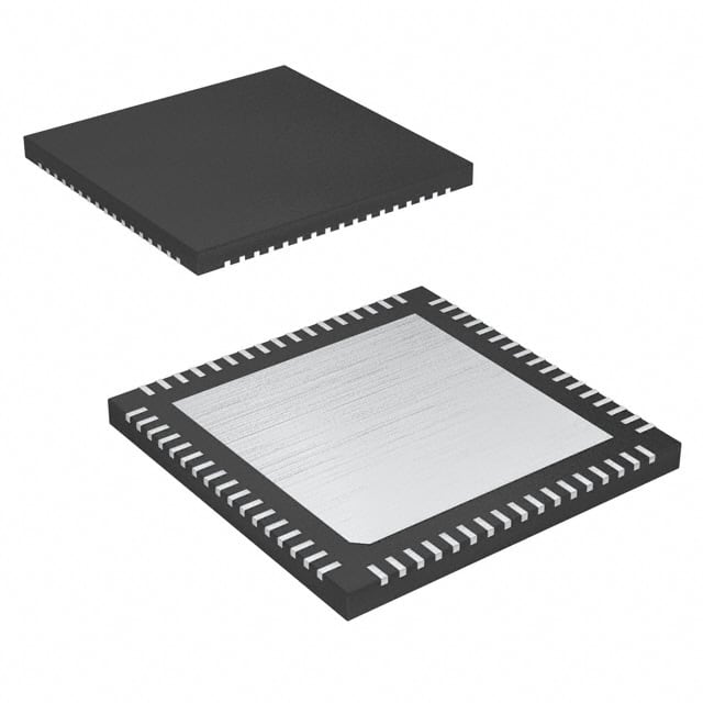
- Part No.:
- MAX14808ETK+T
- Manufacturer:
- Analog Devices Inc./Maxim Integrated
- Category:
- Power Management - Specialized
- Package:
- 68-WFQFN Exposed Pad
- Datasheet:
-
 MAX14808ETK+T.pdf
- Description:
- IC MUX DUAL HV 68TQFN
- Quantity:
- Payment:

- Shipping:

Inventory:770
Please send an inquiry. Send us your inquiry, and we will respond immediately.
Product details
Overview
MAX14808ETK+T from Maxim Integrated is an octal three-level / quad five-level high-voltage digital pulser IC with integrated transmit/receive (T/R) switches, designed for ultrasound transducer driving. It delivers ±105V bipolar pulses at up to 2A peak output current per channel, features embedded active return-to-zero clamping, and operates in clocked or transparent mode with 18ns propagation delay. It targets medical ultrasound imaging systems requiring high-channel-density, low-jitter, and low-power HV pulsing.
For engineers reviewing the MAX14808ETK+T datasheet, MAX14808ETK+T pinout, MAX14808ETK+T application, or MAX14808ETK+T equivalent, key selection considerations include its integrated T/R switch (11.5Ω on-resistance), programmable output current (0.5–2A), DirectDrive® architecture eliminating external HV capacitors, and support for both octal three-level and quad five-level operation modes with differential clock synchronization for Doppler-grade timing integrity.
Technical Context
The MAX14808ETK+T implements a dual-mode pulser architecture: in octal three-level mode, each of eight channels uses two logic inputs (DINN_/DINP_) and provides 1A typical active return-to-zero drive; in quad five-level mode, four channels use three logic inputs and deliver 2A typical return-to-zero drive. Both modes support clocked (differential/single-ended) and transparent operation, with sync functionality reducing FPGA-induced jitter for Doppler applications.
It integrates floating power supplies (FPS), level shifters, grass-clipping diodes (2.5pF reverse capacitance), and a 500Ω active damping circuit that fully discharges internal nodes before diode activation. The device includes thermal shutdown (+145°C threshold, 20°C hysteresis), overvoltage protection diodes per channel, and independent T/R switching (only on MAX14808) with 0.65µs turn-on and 0.02µs turn-off times.
Key Specifications
| Parameter | Value and Actual Design Meaning |
|---|---|
| Output Voltage Range | ±105V (VPP_ to VNN_), enabling direct drive of piezoelectric transducers without external HV amplification stages |
| Peak Output Current | 2A per channel (typical, CC0/CC1 = low/low), supporting high-fidelity burst transmission in B-mode ultrasound |
| Propagation Delay | 18ns (typical), ensuring precise timing alignment across all eight channels for beamforming coherence |
| T/R Switch On-Resistance | 11.5Ω (typical), minimizing signal loss and distortion during receive path isolation |
| THD2 at 5MHz | –43dBc (high-voltage mode), critical for maintaining image contrast and harmonic rejection in diagnostic imaging |
| Quiescent Power per Channel | 5.7mW (octal mode, transparent), enabling portable and battery-operated ultrasound systems |
| Supply Voltage Range (VPP_/VNN_) | –110V to +110V, accommodating wide dynamic range transducer biasing requirements |
Pinout & Package
MAX14808ETK+T is housed in a 68-pin, 10mm × 10mm TQFN package with exposed thermal pad, optimized for high-density PCB layouts in portable ultrasound front-ends.
| Pin/Terminal | Circuit Role | Design Meaning |
|---|---|---|
| VPPA, VPPB | High-side positive HV supply rails | Accept up to +105V; power high-side output stage and internal FPS; require local 1µF bypassing |
| VNNA, VNNB | High-side negative HV supply rails | Accept down to –105V; power low-side output stage and internal FPS; require local 1µF bypassing |
| OUTA–OUTH | Eight high-voltage differential outputs | Deliver three- or five-level bipolar pulses directly to transducer elements; include integrated clamp and damping |
| DINP_A–DINP_H, DINN_A–DINN_H | Logic-level input pairs per channel | Control pulse polarity and level; compatible with 1.7–5.25V logic; 4pF input capacitance minimizes timing skew |
| CLK, CLK | Differential clock input | Enables jitter-reduced clocked mode; supports up to 200MHz; common-mode range centered at VCC/2 |
| LDO_EN | Floating power supply enable | Activates internal LDOs to generate +5V supplies for VGP_/VGN_; reduces need for external regulators |
| MODE0, MODE1 | Operation mode select | Set octal three-level (MODE0=1, MODE1=0), quad five-level (MODE0=0, MODE1=1), or shutdown (both=0) |
| THP | Thermal warning flag | Open-drain output asserted low when junction temperature exceeds +145°C; enables system-level thermal management |
Key Features
| Feature | Design Value |
|---|---|
| Integrated T/R switches | Eight monolithically integrated switches (11.5Ω RON, –50dB crosstalk) eliminate discrete switch arrays and reduce layout complexity |
| DirectDrive® architecture | Removes requirement for external HV coupling capacitors, reducing board area, cost, and reliability risk from capacitor aging/failure |
| Programmable output current | Four-step current control (0.5A/1.0A/1.5A/2.0A) via CC0/CC1 pins allows dynamic power scaling per imaging mode (e.g., lower current in CW Doppler) |
| Active return-to-zero clamp | Embedded nFET/pFET clamp (13.5Ω RONG/ROPG) ensures fast, controlled discharge between pulses-critical for echo fidelity and SNR |
| Differential clock synchronization | Reduces phase noise from FPGA clock outputs by >10dB, directly improving Doppler velocity resolution and spectral purity |
| Grass-clipping diode isolation | Low-parasitic (2.5pF) diodes provide Tx/Rx isolation during receive window, preventing amplifier saturation and enabling high-sensitivity detection |
Applications
| Medical Ultrasound Imaging | Industrial Flaw Detection |
|---|---|
|
Use Scenario: Real-time B-mode and CW Doppler imaging in handheld and cart-based diagnostic systems. IC Role / Device Role / Timing Role: High-voltage pulser and T/R switch controller delivering synchronized ±105V, 2A bursts to 128+ transducer elements with <18ns inter-channel skew. Use Value: Enables high-resolution, low-artifact imaging through precise pulse shaping, low THD2 (–43dBc), and jitter-free clocking for Doppler analysis. |
Use Scenario: Ultrasonic non-destructive testing (NDT) of welds, castings, and composite materials using phased-array probes. IC Role / Device Role / Timing Role: Eight-channel HV driver generating calibrated, repeatable bursts for time-of-flight measurement and defect localization. Use Value: Delivers consistent pulse amplitude and edge fidelity across temperature (–40°C to +85°C), ensuring measurement repeatability in field-deployed NDT equipment. |
| Piezoelectric Actuator Control | Ultrasound Therapy Systems |
|
Use Scenario: Precision positioning and vibration control in microfluidic pumps, nanopositioners, and adaptive optics. IC Role / Device Role / Timing Role: Low-noise, programmable-current HV driver operating in three-level mode for closed-loop waveform synthesis. Use Value: Supports arbitrary waveform generation with 5.7mW/channel quiescent dissipation and 20MHz bandwidth, enabling high-fidelity actuation without thermal drift. |
Use Scenario: High-intensity focused ultrasound (HIFU) ablation systems requiring controlled, high-energy acoustic pulses. IC Role / Device Role / Timing Role: Robust HV pulser with thermal shutdown (+145°C) and active damping, managing duty-cycle-limited burst delivery to therapeutic transducers. Use Value: Ensures safe, repeatable energy delivery via integrated overtemperature protection, fast damping (500Ω), and reliable T/R isolation during treatment cycles. |
Equivalent & Alternatives
The following parts are listed as comparable options for similar high-voltage digital pulser applications.
| Alternative Part | Technical Difference | Application Difference | Selection Advice |
|---|---|---|---|
| MAX14809ETK+T | No integrated T/R switches; identical pulser core, pinout, and electrical specs otherwise | Suitable where external T/R switching is preferred or already implemented; lower channel count per IC required | Select MAX14809ETK+T when T/R integration is unnecessary and board space allows discrete switch placement |
| Texas Instruments TX7332 | 16-channel, 100V max, no integrated T/R switches; requires external FPS and clock conditioning; higher quiescent current (12mW/channel) | Targeted at lower-cost, lower-channel-count industrial ultrasound; lacks DirectDrive® and sync jitter reduction | Choose TX7332 only for cost-sensitive, non-Doppler applications where thermal and timing performance margins are relaxed |
Compared with MAX14808ETK+T, MAX14809ETK+T removes T/R functionality while retaining identical pulser performance and footprint-ideal for modular designs-whereas TX7332 trades integration, jitter suppression, and power efficiency for channel density and cost, making it unsuitable for diagnostic-grade imaging.
Availability
MAX14808ETK+T is available at Aetrix Electronics and suitable for medical ultrasound imaging, industrial flaw detection, and piezoelectric actuator control requiring stable component supply, long-term lifecycle assurance, and traceable sourcing for Class II medical device manufacturing.
Supply support for MAX14808ETK+T includes scheduled delivery planning, volume procurement assistance, BOM continuity management, traceable sourcing, and lifecycle availability coordination for OEM customers, industrial embedded developers, connected-device designers, and electronics production programs.
Manufacturer
Maxim Integrated (now part of Analog Devices) is a leader in precision analog, mixed-signal, and high-voltage interface ICs, serving medical, industrial, and communications markets with robust, application-optimized solutions.
The MAX14808ETK+T belongs to Maxim's ultrasound pulser product line, engineered specifically for high-channel-count, low-jitter, high-fidelity transducer excitation in portable and diagnostic imaging systems-prioritizing THD, timing accuracy, and integration density.
FAQ
What is the maximum high-voltage supply rating for MAX14808ETK+T?
The MAX14808ETK+T supports VPP_ up to +105V and VNNA/VNNB down to –105V, with absolute maximum ratings of +110V and –110V respectively. Operation at ±105V is specified across the full –40°C to +85°C temperature range and enables direct drive of standard medical ultrasound transducers without external HV amplification stages. Exceeding ±105V may compromise THD2 performance and long-term reliability.
Does MAX14808ETK+T require external high-voltage coupling capacitors?
No, MAX14808ETK+T implements Maxim's DirectDrive® architecture, which embeds floating power supplies and level shifters to eliminate the need for external HV coupling capacitors. This reduces PCB area, component count, and failure risks associated with capacitor aging or voltage derating-confirmed in the device's functional description and benefits section.
How does the T/R switch in MAX14808ETK+T improve ultrasound system performance?
The integrated T/R switch in MAX14808ETK+T provides 11.5Ω on-resistance and >60dB off-isolation, enabling fast, low-distortion switching between transmit burst and receive echo windows. Its 0.65µs turn-on and 0.02µs turn-off times minimize dead time, while –50dB crosstalk prevents channel interference-directly enhancing image SNR and spatial resolution in multi-element arrays.
Can MAX14808ETK+T operate in both three-level and five-level pulser modes simultaneously?
No, MAX14808ETK+T operates exclusively in one mode at a time, selected by MODE0/MODE1 pins: octal three-level (MODE0=1, MODE1=0) or quad five-level (MODE0=0, MODE1=1). The device does not support mixed-mode operation; all eight channels follow the same mode configuration, ensuring deterministic timing and consistent power delivery per imaging protocol.
What thermal protection features does MAX14808ETK+T include?
MAX14808ETK+T incorporates thermal shutdown with a +145°C trip threshold and 20°C hysteresis, plus an open-drain THP pin that asserts low when the junction temperature exceeds the threshold. These features protect against sustained overload or poor heatsinking in compact ultrasound modules, and are verified in the Absolute Maximum Ratings and DC Electrical Characteristics tables.
MAX14808ETK+T Specifications
- Product attributes
- Attribute value
- Manufacturer:
- Analog Devices Inc./Maxim Integrated
- Series:
- -
- Package/Case:
- 68-WFQFN Exposed Pad
- Packaging:
- Tape & Reel (TR)
- Product Status:
- Active
- Applications:
- Ultrasound Imaging
- Current - Supply:
- -
- Voltage - Supply:
- 3V, 5V
- Operating Temperature:
- -40°C ~ 85°C
- Grade:
- -
- Qualification:
- -
- Mounting Type:
- Surface Mount
- Supplier Device Package:
- 68-TQFN (10x10)
MAX14808ETK+T FAQ
1.How can I place an order for MAX14808ETK+T through Aetrix?
Please submit a Request for Quotation (RFQ) for MAX14808ETK+T on Aetrix. Our sales agent will provide a competitive quotation and guide you through the order confirmation once you accept the terms.
2.Are the price and stock information for MAX14808ETK+T reliable?
The price and inventory of MAX14808ETK+T are updated periodically and may fluctuate due to market conditions. Stock and pricing data are typically refreshed every 24 hours. Quotation validity for MAX14808ETK+T is usually 5 days.
3.What payment methods are accepted for MAX14808ETK+T?
We accept Wire Transfer, PayPal, Credit Card, Western Union, MoneyGram, and Escrow for MAX14808ETK+T transactions.
Note: Certain payment methods may incur a processing fee.
4.How is shipping managed for MAX14808ETK+T?
MAX14808ETK+T orders can be shipped via leading logistics carriers, including DHL, UPS, FedEx, TNT, or Registered Mail.
Once your MAX14808ETK+T order is processed, you will receive an email with the shipment details and tracking number.
Note: Tracking information may take up to 24 hours to appear. Express delivery typically takes 3–5 business days.
5.How can I obtain technical support or documentation for MAX14808ETK+T?
For technical support, including MAX14808ETK+T datasheets, pinout diagrams, or application guidance, please contact our engineering support team. They can provide detailed documentation and assistance for your MAX14808ETK+T requirements.
6.How does Aetrix verify that MAX14808ETK+T is sourced from the original manufacturer or authorized distributors?
All MAX14808ETK+T products on Aetrix are procured from qualified distributors and authorized channels. Our dedicated quality assurance team conducts strict verification, including traceability checks and, if necessary, third-party testing. This ensures that MAX14808ETK+T meets industry standards.
7.What is the process for return or replacement of MAX14808ETK+T?
All MAX14808ETK+T units undergo pre-shipment inspection (PSI). If there is an issue with MAX14808ETK+T, returns or replacements are accepted under the following conditions:
1.Quantity discrepancies, incorrect items, or visible external defects (such as breakage or corrosion), acknowledged by Aetrix.
2.The issue is reported within 90 days of delivery.
3.The MAX14808ETK+T part is unused and in its original packaging.
Return procedure for MAX14808ETK+T:
1.Submit a request within 90 days.
2.Obtain a Return Material Authorization (RMA) from Aetrix.
MAX14808ETK+T Tags

-
TPS2511DGNR
Texas Instruments

-
UTC2000/MG
Microchip Technology

-
TUSB320HAIRWBR
Texas Instruments

-
TPS61252DSGR
Texas Instruments

-
PI5USB30216CXUAEX
Diodes Incorporated

-
SN6501DBVR
Texas Instruments

-
CYPD3177-24LQXQT
Infineon Technologies
-
SN6501QDBVRQ1
Texas Instruments

-
STUSB1600AQTR
STMicroelectronics

-
SN6505BDBVR
Texas Instruments
-
SN6501DBVT
Texas Instruments

-
TPS65150PWPR
Texas Instruments
Tech Hub

A practical engineering guide to 3.3V and 5V logic compatibility, input thresholds, resistor dividers, translator ICs, MOSFET level shifting, I2C pull-ups, timing limits and power-sequencing risks.

The 74HC595 uses push-pull logic outputs, while the TPIC6B595 uses 50 V open-drain DMOS sinks for higher-power loads. This guide compares timing, current limits, 3.3 V interfacing, load wiring, thermal…

The 74HC595 converts serial data into eight stable parallel outputs. This guide covers pin functions, shift and storage timing, OE and MR behavior, drive-current limits, cascading, voltage compatibilit…

A technical comparison of level-sensitive latches and edge-triggered flip-flops, covering timing windows, setup and hold limits, master–slave operation, time borrowing, race-through, HDL inference and…

A D latch stores one bit while Enable controls when data can pass. This reference covers gate-level operation, truth tables, transparency, setup and hold timing, LE versus OE, common ICs and practical …

An SR latch stores one bit through cross-coupled feedback. This engineering reference covers NOR and NAND implementations, truth tables, forbidden-state recovery, gated operation, switch debouncing, fa…

Latch circuits retain one bit through feedback. This technical reference covers SR and D latches, truth tables, transparency, timing limits, latch-versus-flip-flop behavior, applications and common log…

An engineering guide to LED driver operation, constant-current and constant-voltage outputs, linear and switching topologies, dimming, IC selection, calculations, replacement compatibility, and fault c…

Operational amplifier guide covering op amp basics, feedback, ideal vs real op amps, common configurations, buffer circuits, offset, bias current, gain-bandwidth, slew rate, rail-to-rail limits and sel…

Jumper cables guide covering safe connection order, red and black clamp placement, final ground connection, cable gauge, length, clamp quality, copper vs CCA cables, jump starter comparison and battery…


