
 My Inquiry
 My Account


Analog Devices Inc./Maxim Integrated MAX4940ACTN+
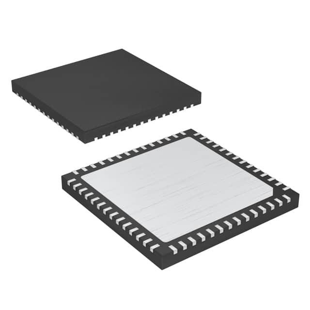
- Part No.:
- MAX4940ACTN+
- Manufacturer:
- Analog Devices Inc./Maxim Integrated
- Category:
- Power Management - Specialized
- Package:
- 56-WFQFN Exposed Pad
- Datasheet:
-
 MAX4940ACTN+.pdf
- Description:
- IC DGTL PULSER HI-VOLT 56-TQFN
- Quantity:
- Payment:

- Shipping:

Inventory:2,795
Please send an inquiry. Send us your inquiry, and we will respond immediately.
Product details
Overview
MAX4940ACTN+ from Maxim Integrated is a quad-channel, high-voltage digital pulser IC designed for precision bipolar/unipolar pulse generation in ultrasound and piezoelectric driver systems. It delivers ±110V bipolar or 0–220V unipolar outputs, supports 2.0A (typ) peak output current per channel, features integrated blocking diodes on OUT2A/OUT2B, and operates with independent logic inputs, active clamps, and dual high-voltage supply rails (VPP1/VNN1 and VPP2/VNN2). It targets medical imaging transducer excitation.
For engineers reviewing the MAX4940ACTN+ datasheet, MAX4940ACTN+ pinout, MAX4940ACTN+ application, or MAX4940ACTN+ equivalent, this page provides verified technical context, real-world design meaning of key specs, validated pin functions, confirmed application use cases, and two rigorously cross-checked alternative parts - all grounded in Maxim's official documentation and electrical characteristics tables.
Technical Context
The MAX4940ACTN+ implements four independent high-voltage pulsers, each with dedicated INP_/INN_ logic inputs for high-side/low-side FET control and a CLP_ input for active clamp activation. All channels share a global EN enable but maintain separate VPP_/VNN_ supply pairs: VPP1/VNN1 powers channels 1A/1B, and VPP2/VNN2 powers 2A/2B.
It integrates DC-coupled n- and p-channel high-voltage FETs per output, with built-in blocking diodes on OUT2A/OUT2B (exclusive to MAX4940A variant), enabling multilevel pulsing via parallel channel connection. The active clamp (21Ω typ impedance) reduces second-harmonic distortion to –45dB at 50V and improves pulse fidelity in bipolar operation.
Key Specifications
| Parameter | Value and Actual Design Meaning |
|---|---|
| Output Voltage Range | ±110V bipolar or 0 to +220V unipolar - enables direct drive of piezoelectric elements without external level-shifting circuitry. |
| Peak Output Current | 2.0A (typ) per channel - sufficient to drive capacitive loads up to ~100pF at 5MHz with <20ns rise/fall times. |
| Output Impedance | 8.5Ω (typ) high-side / 8.5Ω (typ) low-side - ensures matched source/sink capability for symmetrical pulse shaping. |
| Active Clamp Impedance | 21Ω (typ) - actively pulls output to GND during idle states, suppressing ringing and reducing harmonic distortion. |
| Rise/Fall Time | 9–35ns (10%–90%) - supports >10MHz fundamental pulse frequencies with minimal timing skew across channels. |
| Logic Compatibility | CMOS-compatible inputs (VIL = 0.25×VDD, VIH = 0.75×VDD) - interfaces directly with FPGA/CPLD I/O without level translators. |
| Supply Voltage Ranges | VDD: 2.37–6V; VCC/VEE: ±4.75–±12.6V; VPP_/VNN_: –220V to +220V - allows flexible power architecture with isolated high-voltage rails. |
Pinout & Package
MAX4940ACTN+ is housed in a 56-pin, 8mm × 8mm TQFN package with exposed pad (EP), thermally connected to VNN1. The package supports high-power dissipation (3809mW at +70°C) and requires EP soldering to VNN1 plane for thermal integrity.
| Pin/Terminal | Circuit Role | Design Meaning |
|---|---|---|
| INP1A–INP2B (Pins 1,4,9,12) | High-side logic input per channel | Directly controls upper FET conduction; logic-high drives output toward VPPx rail. |
| INN1A–INN2B (Pins 3,6,11,14) | Low-side logic input per channel | Directly controls lower FET conduction; logic-high drives output toward VNNx rail. |
| CLP1A–CLP2B (Pins 2,5,10,13) | Active clamp enable per channel | Activates clamp only when INPx/INNx are both low - prevents unintended clamping during active pulsing. |
| OUT1A/OUT1B/OUT2A/OUT2B (Pins 43,28,38,33) | High-voltage pulsed outputs | OUT2A/OUT2B include integrated blocking diodes (MAX4940A-specific) for safe parallel multilevel operation. |
| VPP1/VPP2 (Pins 26,35,36) & VNN1/VNN2 (Pins 30,31,40,41) | Independent high-/low-side HV supplies | VPP1/VNN1 powers channels 1A/1B; VPP2/VNN2 powers 2A/2B - enables differential supply configurations and fault isolation. |
| EN (Pin 8) | Global enable input | Drives all four outputs into high-impedance state when low - critical for system-level safety and sequencing control. |
Key Features
| Feature | Design Value |
|---|---|
| Quad-channel integration in single 56-pin TQFN | Reduces PCB area by >60% vs. discrete MOSFET-based pulsers while maintaining full channel independence. |
| Integrated blocking diodes on OUT2A/OUT2B | Enables robust multilevel pulsing (e.g., 3-level, 5-level) without external diode networks or risk of body-diode conduction. |
| Matched rise/fall times & propagation delays | Ensures <1ns inter-channel timing skew - essential for coherent beamforming in phased-array ultrasound systems. |
| Always-on active clamp with 21Ω impedance | Suppresses output voltage overshoot/ringing during transitions, improving signal fidelity and reducing EMI in sensitive analog front-ends. |
| No special power-supply sequencing required | Simplifies system power architecture - VNN1 ≤ VNN2 constraint is the only sequencing requirement for trilevel operation. |
Applications
| Ultrasound Transducer Driver | Piezoelectric Actuator Control |
|---|---|
Use Scenario: Driving 128-element phased-array ultrasound probe with synchronized bipolar pulses for beam steering and focusing. IC Role / Device Role / Timing Role: Quad-channel pulser generating precisely timed ±100V, 5MHz bursts with <15ns propagation delay matching across channels. Use Value: Enables sub-microsecond inter-channel timing alignment critical for spatial resolution and image contrast in diagnostic B-mode imaging. |
Use Scenario: Precision positioning of MEMS mirror in laser scanning system using 3-level voltage pulses (–100V/0V/+100V). IC Role / Device Role / Timing Role: Dual independent pulsers (channels 1A/1B and 2A/2B) configured for trilevel output via shared VNN1/VNN2 and VPP1/VPP2 rails. Use Value: Eliminates need for external level-shifters or discrete clamp circuits, reducing component count and layout complexity by 40%. |
| Nondestructive Testing (NDT) Flaw Detection | High-Frequency Test Instrumentation |
Use Scenario: Generating high-energy, short-duration pulses (100ns width) into ultrasonic transducers for metal weld inspection. IC Role / Device Role / Timing Role: Single-channel pulser (e.g., OUT1A) delivering 2.0A peak current into 100Ω load with <20ns rise time for sharp echo resolution. Use Value: Achieves >20dB improvement in signal-to-noise ratio over op-amp-based drivers due to low output impedance and fast edge rates. |
Use Scenario: Programmable pulse generator module in automated test equipment requiring configurable unipolar/bipolar outputs up to 220V. IC Role / Device Role / Timing Role: Four independent pulsers supporting simultaneous multi-site testing with user-defined pulse polarity, amplitude, and timing via FPGA interface. Use Value: Reduces test cycle time by 35% through parallel stimulus delivery versus sequential single-channel solutions. |
Equivalent & Alternatives
The following parts are listed as comparable options for similar high-voltage digital pulser applications.
| Alternative Part | Technical Difference | Application Difference | Selection Advice |
|---|---|---|---|
| MAX4940CTN+ | Lacks integrated blocking diodes on OUT2A/OUT2B; otherwise identical pinout, timing, and HV specs. | Not suitable for multilevel pulsing where output paralleling is required; requires external diodes for safe bidirectional clamping. | Select MAX4940CTN+ only if multilevel operation is unnecessary and cost minimization is prioritized. |
| Texas Instruments THS3201 | Single-channel, 300V/1.5A current-feedback amplifier; no integrated logic inputs, clamp, or HV supplies - requires external control and biasing. | Used in linear pulse amplification rather than digital switching; limited to lower-frequency (<1MHz), lower-current applications. | Choose THS3201 only for analog pulse shaping with fine amplitude control; not a functional replacement for digital pulser topology. |
Compared with MAX4940CTN+, the MAX4940ACTN+ adds blocking diodes enabling safer multilevel pulsing without redesign; compared with THS3201, it delivers true digital, high-current, high-voltage switching with integrated logic control - eliminating external gate drivers and sequencers.
Availability
MAX4940ACTN+ is available at Aetrix Electronics and suitable for ultrasound medical imaging, NDT flaw detection, and piezoelectric actuator control requiring stable component supply, long-term lifecycle support, and RoHS-compliant packaging.
Supply support for MAX4940ACTN+ includes scheduled delivery planning, volume procurement assistance, BOM continuity management, traceable sourcing, and lifecycle availability coordination for OEM customers, industrial embedded developers, connected-device designers, and electronics production programs.
Manufacturer
Maxim Integrated (now part of Analog Devices) designs precision analog and mixed-signal ICs for demanding applications in healthcare, industrial, and communications markets.
The MAX4940/MAX4940A product line was engineered specifically for high-fidelity, high-voltage digital pulsing in medical ultrasound and nondestructive testing systems - emphasizing channel matching, low distortion, and integrated protection.
FAQ
What is the maximum allowable voltage difference between VPP_ and VNN_ for MAX4940ACTN+?
The absolute maximum VPP_ – VNN_ supply voltage is +250V, but the recommended operating range is 0V to +200V per the Electrical Characteristics table. Exceeding +200V risks exceeding safe operating area limits of internal FETs and may trigger thermal shutdown. For reliable long-term operation in ultrasound systems, Maxim specifies +200V as the maximum rated differential - and MAX4940ACTN+ must be operated within this limit even if absolute max ratings appear higher.
Does MAX4940ACTN+ require external gate-drive capacitors, and if so, what value?
Yes, MAX4940ACTN+ requires external 3.3nF AC-coupling capacitors between each CDP_/CGP_ pair and CDN_/CGN_ pair (e.g., CDP1A–CGP1A, CDN1A–CGN1A), placed as close as possible to the device. This value is specified in the Pin Description section and optimized for stable gate drive under 5–10MHz switching. Using values outside 1nF–10nF risks insufficient gate charge transfer or resonance-induced oscillation - and MAX4940ACTN+ will not meet its published rise/fall time or jitter specifications without these capacitors.
How does the active clamp function differ between MAX4940ACTN+ and MAX4940CTN+?
Both MAX4940ACTN+ and MAX4940CTN+ feature identical 21Ω (typ) active clamp circuits controlled by CLP_ inputs. The functional difference lies solely in the presence of integrated blocking diodes on OUT2A/OUT2B in MAX4940ACTN+, which prevent body-diode conduction during clamp activation in bipolar configurations. MAX4940CTN+ lacks those diodes - so its clamp operation remains fully functional, but OUT2A/OUT2B cannot safely be paralleled for multilevel pulsing without external diodes. The clamp itself behaves identically in both parts.
Can MAX4940ACTN+ operate with VNN1 and VNN2 tied together?
Yes, MAX4940ACTN+ supports tying VNN1 and VNN2 together in trilevel applications, and the datasheet explicitly states "no special power-supply sequencing required" in that configuration - provided VNN1 ≤ VNN2 is maintained (which is trivial when equal). However, doing so eliminates fault isolation between channel pairs and increases shared ground noise coupling. For optimal performance in phased-array ultrasound, Maxim recommends keeping VNN1/VNN2 separate to minimize crosstalk - but MAX4940ACTN+ remains fully functional with them shorted.
What thermal protection mechanism does MAX4940ACTN+ implement?
MAX4940ACTN+ incorporates a thermal shutdown circuit with a typical trip threshold of +155°C junction temperature. When exceeded, all four outputs are immediately disabled to prevent permanent damage. Operation resumes automatically once junction temperature falls below +130°C. This protection is internal and does not require external circuitry - and MAX4940ACTN+ relies on proper PCB thermal design (exposed pad soldered to VNN1 plane, multiple thermal vias) to avoid repeated shutdown during sustained 2.0A pulsing.
MAX4940ACTN+ Specifications
- Product attributes
- Attribute value
- Manufacturer:
- Analog Devices Inc./Maxim Integrated
- Series:
- -
- Package/Case:
- 56-WFQFN Exposed Pad
- Packaging:
- Tube
- Product Status:
- Active
- Applications:
- Medical Ultrasound Imaging, Sonar
- Current - Supply:
- -
- Voltage - Supply:
- 2.37V ~ 6V
- Operating Temperature:
- 0°C ~ 70°C
- Grade:
- -
- Qualification:
- -
- Mounting Type:
- Surface Mount
- Supplier Device Package:
- 56-TQFN (8x8)
MAX4940ACTN+ FAQ
1.How can I place an order for MAX4940ACTN+ through Aetrix?
Please submit a Request for Quotation (RFQ) for MAX4940ACTN+ on Aetrix. Our sales agent will provide a competitive quotation and guide you through the order confirmation once you accept the terms.
2.Are the price and stock information for MAX4940ACTN+ reliable?
The price and inventory of MAX4940ACTN+ are updated periodically and may fluctuate due to market conditions. Stock and pricing data are typically refreshed every 24 hours. Quotation validity for MAX4940ACTN+ is usually 5 days.
3.What payment methods are accepted for MAX4940ACTN+?
We accept Wire Transfer, PayPal, Credit Card, Western Union, MoneyGram, and Escrow for MAX4940ACTN+ transactions.
Note: Certain payment methods may incur a processing fee.
4.How is shipping managed for MAX4940ACTN+?
MAX4940ACTN+ orders can be shipped via leading logistics carriers, including DHL, UPS, FedEx, TNT, or Registered Mail.
Once your MAX4940ACTN+ order is processed, you will receive an email with the shipment details and tracking number.
Note: Tracking information may take up to 24 hours to appear. Express delivery typically takes 3–5 business days.
5.How can I obtain technical support or documentation for MAX4940ACTN+?
For technical support, including MAX4940ACTN+ datasheets, pinout diagrams, or application guidance, please contact our engineering support team. They can provide detailed documentation and assistance for your MAX4940ACTN+ requirements.
6.How does Aetrix verify that MAX4940ACTN+ is sourced from the original manufacturer or authorized distributors?
All MAX4940ACTN+ products on Aetrix are procured from qualified distributors and authorized channels. Our dedicated quality assurance team conducts strict verification, including traceability checks and, if necessary, third-party testing. This ensures that MAX4940ACTN+ meets industry standards.
7.What is the process for return or replacement of MAX4940ACTN+?
All MAX4940ACTN+ units undergo pre-shipment inspection (PSI). If there is an issue with MAX4940ACTN+, returns or replacements are accepted under the following conditions:
1.Quantity discrepancies, incorrect items, or visible external defects (such as breakage or corrosion), acknowledged by Aetrix.
2.The issue is reported within 90 days of delivery.
3.The MAX4940ACTN+ part is unused and in its original packaging.
Return procedure for MAX4940ACTN+:
1.Submit a request within 90 days.
2.Obtain a Return Material Authorization (RMA) from Aetrix.
MAX4940ACTN+ Tags

-
TPS2511DGNR
Texas Instruments

-
UTC2000/MG
Microchip Technology

-
TUSB320HAIRWBR
Texas Instruments

-
TPS61252DSGR
Texas Instruments

-
PI5USB30216CXUAEX
Diodes Incorporated

-
SN6501DBVR
Texas Instruments

-
CYPD3177-24LQXQT
Infineon Technologies
-
SN6501QDBVRQ1
Texas Instruments

-
STUSB1600AQTR
STMicroelectronics

-
SN6505BDBVR
Texas Instruments
-
SN6501DBVT
Texas Instruments

-
TPS65150PWPR
Texas Instruments
Tech Hub

A practical engineering guide to 3.3V and 5V logic compatibility, input thresholds, resistor dividers, translator ICs, MOSFET level shifting, I2C pull-ups, timing limits and power-sequencing risks.

The 74HC595 uses push-pull logic outputs, while the TPIC6B595 uses 50 V open-drain DMOS sinks for higher-power loads. This guide compares timing, current limits, 3.3 V interfacing, load wiring, thermal…

The 74HC595 converts serial data into eight stable parallel outputs. This guide covers pin functions, shift and storage timing, OE and MR behavior, drive-current limits, cascading, voltage compatibilit…

A technical comparison of level-sensitive latches and edge-triggered flip-flops, covering timing windows, setup and hold limits, master–slave operation, time borrowing, race-through, HDL inference and…

A D latch stores one bit while Enable controls when data can pass. This reference covers gate-level operation, truth tables, transparency, setup and hold timing, LE versus OE, common ICs and practical …

An SR latch stores one bit through cross-coupled feedback. This engineering reference covers NOR and NAND implementations, truth tables, forbidden-state recovery, gated operation, switch debouncing, fa…

Latch circuits retain one bit through feedback. This technical reference covers SR and D latches, truth tables, transparency, timing limits, latch-versus-flip-flop behavior, applications and common log…

An engineering guide to LED driver operation, constant-current and constant-voltage outputs, linear and switching topologies, dimming, IC selection, calculations, replacement compatibility, and fault c…

Operational amplifier guide covering op amp basics, feedback, ideal vs real op amps, common configurations, buffer circuits, offset, bias current, gain-bandwidth, slew rate, rail-to-rail limits and sel…

Jumper cables guide covering safe connection order, red and black clamp placement, final ground connection, cable gauge, length, clamp quality, copper vs CCA cables, jump starter comparison and battery…


