
 My Inquiry
 My Account


Microchip Technology MD1730-I/M2
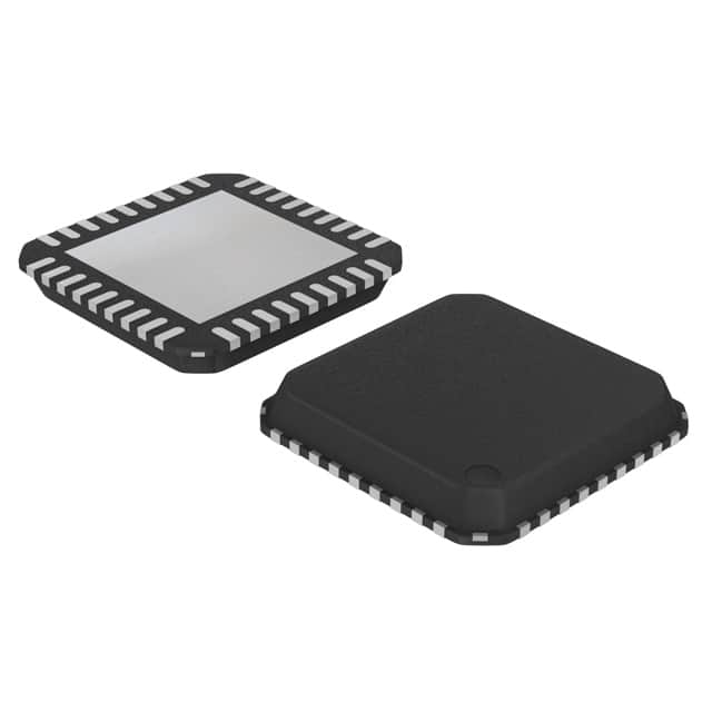
- Part No.:
- MD1730-I/M2
- Manufacturer:
- Microchip Technology
- Category:
- Power Management - Specialized
- Package:
- 36-VFQFN Exposed Pad
- Datasheet:
-
 MD1730-I/M2.pdf
- Description:
- IC ULTRASOUND IMAGING 36VQFN
- Quantity:
- Payment:

- Shipping:

Inventory:4,599
Please send an inquiry. Send us your inquiry, and we will respond immediately.
Product details
Overview
MD1730-I/M2 from Microchip Technology is an 8-channel ultra-low phase noise continuous waveform (CW) transmitter with integrated digital beamformer, designed for medical ultrasound Doppler systems. It delivers ±1V to ±6Vp-p CW output swing, supports input clock frequencies up to 250 MHz, and achieves −160 dBc/Hz phase noise at 1 kHz offset from a 5 MHz carrier - enabling high-fidelity cardiovascular imaging and fetal heart monitoring.
For engineers reviewing the MD1730-I/M2 datasheet, MD1730-I/M2 pinout, MD1730-I/M2 application, or MD1730-I/M2 equivalent, key selection criteria include per-channel 8-bit programmable phase delay resolution (down to 6.25 ns at 160 MHz clock), SPI-controlled frequency division across all eight outputs, LVDS/SSTL/LVCMOS clock compatibility, and thermal management via exposed pad in VQFN package.
Technical Context
The MD1730-I/M2 implements a dedicated low-noise analog signal path with matched PFET/NFET output stages (RON = 7.5 Ω / 6.5 Ω typ.), minimizing jitter accumulation from clock input to CW output. Its dual independent clock buffers (CKB0/CKB1) operate up to 250 MHz and are enabled separately via CBE0/CBE1 - decoupling timing distribution from device enable control.
Beamforming is executed digitally via SPI-writable PHDCH[7:0] registers (256-step delay per channel) and CWFD[7:0] dividers (fCW = fCLK/(2×CWFD), range fCLK/512 to fCLK/2). All eight CW outputs share the same frequency but support independent phase alignment - critical for coherent multi-element transducer excitation.
Key Specifications
| Parameter | Value and Actual Design Meaning |
|---|---|
| CW Output Swing | ±1 V to ±6 Vp-p: Enables direct drive of high-voltage ultrasound transducers without external level-shifting amplifiers. |
| Phase Noise | −160 dBc/Hz @ 1 kHz offset, 5 MHz carrier: Meets stringent spectral purity requirements for Doppler velocity discrimination in cardiac imaging. |
| SPI Speed | Up to 200 MHz: Supports rapid reconfiguration of beamformer parameters during real-time scan mode switching. |
| Input Clock Range | 40–250 MHz (LVDS/SSTL/LVCMOS): Allows flexible system clock architecture with single-source synchronization across multiple MD1730-I/M2 devices. |
| Per-Channel Phase Resolution | 6.25 ns step @ 160 MHz clock (11.25° angular resolution): Enables fine-grained spatial focusing in phased-array ultrasound systems. |
| Output Channel Count | 8 independent CW outputs (CW0–CW7): Matches standard 1:1 channel count for 8-element linear or sector transducer arrays. |
| Supply Voltages | VLL = 2.5 V, VDD = 5 V, VGP = +10 V, VGN = −10 V, VCW+ = +1 to +6 V, VCW− = −1 to −6 V: Segregated power domains isolate logic, analog, and HV output stages. |
Pinout & Package
MD1730-I/M2 is housed in a 36-lead, 6 mm × 6 mm × 0.9 mm VQFN package with exposed thermal pad (EP), optimized for high-power CW transmission and thermal dissipation in compact medical modules.
| Pin/Terminal | Circuit Role | Design Meaning |
|---|---|---|
| EN | Global device enable | Assert high to activate SPI interface and internal regulators; clock buffers remain operational regardless of EN state. |
| CLKP/CLKN | Differential clock input | Accepts LVDS/SSTL signals; supports single-ended LVCMOS 2.5 V with external termination per Figure 4-8. |
| SCK/CSN/SDI/SDO | SPI interface | 200 MHz-capable 4-wire interface; SDO supports daisy-chaining and broadcast mode when SPIB = 1. |
| TXRW | Transmission trigger | High pulse initiates synchronized CW output on all enabled channels; disables SPI access during transmission. |
| CBE0/CBE1 | Independent clock buffer enables | Each controls one 2.5 V single-ended buffered clock output (CKB0/CKB1); no dependency on EN pin. |
| CW0–CW7 | High-voltage CW outputs | Eight fully independent ±6 Vp-p outputs with per-channel programmable phase delay and high-Z disable. |
| VLL/VDD/VGP/VGN/VCW+/VCW− | Power supply rails | Five isolated supplies: logic (2.5 V), core (5 V), positive HV bias (+10 V), negative HV bias (−10 V), and programmable CW output rails (±1 to ±6 V). |
| CPF/CNF | Floating supply bypass | Connect 1 µF/10 V capacitors between CPF↔VCW+ and CNF↔VCW− to stabilize HV output stage regulation. |
Key Features
| Feature | Design Value |
|---|---|
| Ultra-low phase noise architecture | −160 dBc/Hz @ 1 kHz offset enables sub-mm Doppler velocity resolution in echocardiography applications. |
| 8-bit per-channel phase delay | 256-step programmability (0–255/fCLK) allows precise time-aligned excitation across transducer elements for dynamic beam steering. |
| Dual independent clock buffers | CKB0/CKB1 outputs reduce need for external clock fanout ICs, lowering BOM cost and PCB area in multi-chip ultrasound front-ends. |
| SPI daisy-chain & broadcast modes | Single write transaction updates identical registers across multiple MD1730-I/M2 devices - essential for scalable 64+ channel systems. |
| Programmable CW frequency division | 8-bit CWFD register sets identical fCW across all 8 outputs (fCW = fCLK/(2×CWFD)), simplifying multi-frequency Doppler mode implementation. |
Applications
| Cardiovascular Ultrasound Imaging | Fetal Heart Rate Monitoring |
|---|---|
|
Use Scenario: Real-time B-mode and color Doppler imaging of heart valves, chambers, and blood flow dynamics. IC Role / Device Role / Timing Role: Primary CW transmitter generating synchronized 2–10 MHz excitation waveforms across 8 transducer elements with sub-nanosecond inter-channel timing alignment. Use Value: −160 dBc/Hz phase noise ensures accurate spectral analysis of low-velocity blood flow (<5 cm/s), critical for detecting regurgitant jets and diastolic dysfunction. |
Use Scenario: Portable handheld device acquiring fetal heart rate and motion via CW Doppler from maternal abdomen. IC Role / Device Role / Timing Role: Low-power CW source driving miniaturized piezoelectric transducers; uses VLL = 2.5 V and minimal supply currents (2.5 mA typ. at 5 MHz CW). Use Value: Integrated beamformer eliminates external FPGA-based delay logic, reducing system latency and power consumption in battery-operated monitors. |
| Ultrasound Flow Metering | Programmable Array Pattern Generator |
|
Use Scenario: Industrial non-invasive flow measurement in pipes using transit-time or Doppler shift principles. IC Role / Device Role / Timing Role: High-stability CW source providing repeatable 1–5 MHz excitation with <±0.5 ns channel-to-channel delay matching (tdm). Use Value: Matched RON (7.5 Ω PFET / 6.5 Ω NFET) and low ∆RON/°C ensure consistent amplitude and phase response over temperature - vital for calibration stability. |
Use Scenario: Lab equipment generating arbitrary CW patterns for transducer characterization and acoustic field mapping. IC Role / Device Role / Timing Role: Programmable waveform engine supporting independent frequency (via CWFD) and phase (via PHDCH) per channel for synthetic aperture testing. Use Value: SPI broadcast mode allows simultaneous update of 8-channel phase/frequency settings across multiple MD1730-I/M2 units - accelerating test sequence execution. |
Equivalent & Alternatives
The following parts are listed as comparable options for similar CW transmitter applications.
| Alternative Part | Technical Difference | Application Difference | Selection Advice |
|---|---|---|---|
| Texas Instruments AFE5809 | Integrated 8-channel LNA/VGA/ADC; CW transmit capability limited to auxiliary outputs with lower voltage swing (±2.5 V) and higher phase noise (−145 dBc/Hz). | Targeted at receive-focused systems requiring full analog front-end integration; not optimized for standalone high-fidelity CW excitation. | Select AFE5809 only if combined RX/TX functionality and digitization are required on single chip; MD1730-I/M2 preferred for pure high-performance CW generation. |
| Analog Devices AD9106 | 4-channel DAC-based arbitrary waveform generator; CW output derived from digital synthesis with typical phase noise −135 dBc/Hz @ 1 kHz. | Designed for flexible pattern generation (not dedicated CW); lacks integrated beamformer and HV output drivers. | Choose AD9106 for multi-tone or modulated CW synthesis; MD1730-I/M2 delivers superior phase noise and native 8-channel beamforming for clinical ultrasound. |
Compared with AFE5809 and AD9106, MD1730-I/M2 provides the lowest phase noise, highest CW output voltage, and hardware-accelerated beamforming - making it the optimal choice for medical-grade Doppler transmitters where spectral purity and timing precision are non-negotiable.
Availability
MD1730-I/M2 is available at Aetrix Electronics and suitable for cardiovascular ultrasound imaging systems, fetal monitoring devices, and industrial flow metering applications requiring stable component supply, long-term medical-grade qualification, and traceable sourcing.
Supply support for MD1730-I/M2 includes scheduled delivery planning, volume procurement assistance, BOM continuity management, traceable sourcing, and lifecycle availability coordination for OEM customers, industrial embedded developers, connected-device designers, and electronics production programs.
Manufacturer
Microchip Technology is a global semiconductor company specializing in microcontrollers, analog devices, and timing solutions, with deep expertise in medical, automotive, and industrial markets.
The MD1730-I/M2 belongs to Microchip's high-performance ultrasound transmitter product line, engineered specifically for clinical and portable Doppler systems demanding ultra-low phase noise, precise beamforming, and robust HV output drive capability.
FAQ
What is the maximum clock frequency supported by the MD1730-I/M2 for its internal system clock?
The MD1730-I/M2 supports an input clock frequency range of 40 MHz to 250 MHz on its CLKP/CLKN differential inputs. This applies to both LVDS and SSTL signaling standards, and the device also accepts single-ended LVCMOS 2.5 V clocks with appropriate termination. At 250 MHz, the MD1730-I/M2 achieves its highest CW frequency resolution and finest phase delay granularity.
How does the MD1730-I/M2 implement per-channel phase delay control?
The MD1730-I/M2 uses eight independent 8-bit PHDCH[7:0] registers (PHD0 through PHD7), each controlling the delay of one CW output (CW0–CW7). Delay time equals PHDCH/fCLK + 2/fCLK, yielding 6.25 ns resolution at 160 MHz clock. This enables precise electronic beam steering without external delay lines - a core function of the MD1730-I/M2 beamformer.
Can the MD1730-I/M2 generate different CW frequencies on different output channels?
No. The MD1730-I/M2 uses a single 8-bit CWFD[7:0] register to set the frequency divider for all eight CW outputs. As stated in the datasheet, "The selected CW frequency is same for all the CW0~7 outputs." Therefore, MD1730-I/M2 generates identical CW frequencies across all channels, though phase alignment remains independently programmable per channel.
What is the purpose of the CPF and CNF pins on the MD1730-I/M2?
The CPF (Positive Floating Supply Bypass) and CNF (Negative Floating Supply Bypass) pins on the MD1730-I/M2 connect to external 1 µF/10 V capacitors placed between CPF↔VCW+ and CNF↔VCW−. These capacitors stabilize the floating high-voltage supplies that drive the CW output stage, ensuring low-noise regulation and preventing supply-induced phase modulation - a critical design requirement confirmed in MD1730-I/M2 electrical characterization.
Does the MD1730-I/M2 require external high-voltage power supplies?
Yes. The MD1730-I/M2 requires five distinct supply rails: VLL = +2.5 V (logic), VDD = +5 V (core), VGP = +10 V (positive HV bias), VGN = −10 V (negative HV bias), and programmable VCW+ / VCW− (±1 V to ±6 V for CW output swing). These must be provided externally; the MD1730-I/M2 does not include on-chip DC-DC conversion for the HV supplies.
MD1730-I/M2 Specifications
- Product attributes
- Attribute value
- Manufacturer:
- Microchip Technology
- Series:
- -
- Package/Case:
- 36-VFQFN Exposed Pad
- Packaging:
- Tray
- Product Status:
- Obsolete
- Applications:
- Ultrasound Imaging
- Current - Supply:
- -
- Voltage - Supply:
- 4.75V ~ 5.25V
- Operating Temperature:
- 0°C ~ 85°C
- Grade:
- -
- Qualification:
- -
- Mounting Type:
- Surface Mount
- Supplier Device Package:
- 36-SQFN (6x6)
MD1730-I/M2 FAQ
1.How can I place an order for MD1730-I/M2 through Aetrix?
Please submit a Request for Quotation (RFQ) for MD1730-I/M2 on Aetrix. Our sales agent will provide a competitive quotation and guide you through the order confirmation once you accept the terms.
2.Are the price and stock information for MD1730-I/M2 reliable?
The price and inventory of MD1730-I/M2 are updated periodically and may fluctuate due to market conditions. Stock and pricing data are typically refreshed every 24 hours. Quotation validity for MD1730-I/M2 is usually 5 days.
3.What payment methods are accepted for MD1730-I/M2?
We accept Wire Transfer, PayPal, Credit Card, Western Union, MoneyGram, and Escrow for MD1730-I/M2 transactions.
Note: Certain payment methods may incur a processing fee.
4.How is shipping managed for MD1730-I/M2?
MD1730-I/M2 orders can be shipped via leading logistics carriers, including DHL, UPS, FedEx, TNT, or Registered Mail.
Once your MD1730-I/M2 order is processed, you will receive an email with the shipment details and tracking number.
Note: Tracking information may take up to 24 hours to appear. Express delivery typically takes 3–5 business days.
5.How can I obtain technical support or documentation for MD1730-I/M2?
For technical support, including MD1730-I/M2 datasheets, pinout diagrams, or application guidance, please contact our engineering support team. They can provide detailed documentation and assistance for your MD1730-I/M2 requirements.
6.How does Aetrix verify that MD1730-I/M2 is sourced from the original manufacturer or authorized distributors?
All MD1730-I/M2 products on Aetrix are procured from qualified distributors and authorized channels. Our dedicated quality assurance team conducts strict verification, including traceability checks and, if necessary, third-party testing. This ensures that MD1730-I/M2 meets industry standards.
7.What is the process for return or replacement of MD1730-I/M2?
All MD1730-I/M2 units undergo pre-shipment inspection (PSI). If there is an issue with MD1730-I/M2, returns or replacements are accepted under the following conditions:
1.Quantity discrepancies, incorrect items, or visible external defects (such as breakage or corrosion), acknowledged by Aetrix.
2.The issue is reported within 90 days of delivery.
3.The MD1730-I/M2 part is unused and in its original packaging.
Return procedure for MD1730-I/M2:
1.Submit a request within 90 days.
2.Obtain a Return Material Authorization (RMA) from Aetrix.
MD1730-I/M2 Tags

-
TPS2511DGNR
Texas Instruments

-
UTC2000/MG
Microchip Technology

-
TUSB320HAIRWBR
Texas Instruments

-
TPS61252DSGR
Texas Instruments

-
PI5USB30216CXUAEX
Diodes Incorporated

-
SN6501DBVR
Texas Instruments

-
CYPD3177-24LQXQT
Infineon Technologies
-
SN6501QDBVRQ1
Texas Instruments

-
STUSB1600AQTR
STMicroelectronics

-
SN6505BDBVR
Texas Instruments
-
SN6501DBVT
Texas Instruments

-
TPS65150PWPR
Texas Instruments
Tech Hub

TTL and CMOS logic families differ in thresholds, loading, output drive, power and timing. This engineering guide compares 74HC and 74HCT, calculates noise margins and checks 3.3 V/5 V compatibility.

A practical engineering guide to 3.3V and 5V logic compatibility, input thresholds, resistor dividers, translator ICs, MOSFET level shifting, I2C pull-ups, timing limits and power-sequencing risks.

The 74HC595 uses push-pull logic outputs, while the TPIC6B595 uses 50 V open-drain DMOS sinks for higher-power loads. This guide compares timing, current limits, 3.3 V interfacing, load wiring, thermal…

The 74HC595 converts serial data into eight stable parallel outputs. This guide covers pin functions, shift and storage timing, OE and MR behavior, drive-current limits, cascading, voltage compatibilit…

A technical comparison of level-sensitive latches and edge-triggered flip-flops, covering timing windows, setup and hold limits, master–slave operation, time borrowing, race-through, HDL inference and…

A D latch stores one bit while Enable controls when data can pass. This reference covers gate-level operation, truth tables, transparency, setup and hold timing, LE versus OE, common ICs and practical …

An SR latch stores one bit through cross-coupled feedback. This engineering reference covers NOR and NAND implementations, truth tables, forbidden-state recovery, gated operation, switch debouncing, fa…

Latch circuits retain one bit through feedback. This technical reference covers SR and D latches, truth tables, transparency, timing limits, latch-versus-flip-flop behavior, applications and common log…

An engineering guide to LED driver operation, constant-current and constant-voltage outputs, linear and switching topologies, dimming, IC selection, calculations, replacement compatibility, and fault c…

Operational amplifier guide covering op amp basics, feedback, ideal vs real op amps, common configurations, buffer circuits, offset, bias current, gain-bandwidth, slew rate, rail-to-rail limits and sel…


