
 My Inquiry
 My Account


NXP Semiconductors MM912J637AM2EPR2
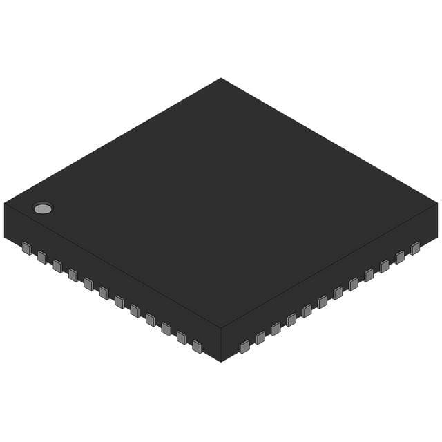
- Part No.:
- MM912J637AM2EPR2
- Manufacturer:
- NXP Semiconductors
- Category:
- Application Specific Microcontrollers
- Package:
- -
- Datasheet:
-
 MM912J637AM2EPR2.pdf
- Description:
- POWER SUPPLY MANAGEMENT CIRCUIT,
- Quantity:
- Payment:

- Shipping:

Inventory:22,000
Please send an inquiry. Send us your inquiry, and we will respond immediately.
Product details
Overview
MM912J637AM2EPR2 from NXP Semiconductors (formerly Freescale) is an intelligent integrated precision battery sensor combining a 128 kB S12 MCU die and analog sensing die in a single 48-pin QFN-EP package. It performs high-accuracy battery voltage measurement (±0.5% full-scale), current sensing via external shunt (8-range PGA with auto-gain control), and on-chip temperature monitoring - all optimized for 12 V lead-acid battery systems in automotive body electronics.
For engineers reviewing the MM912J637AM2EPR2 datasheet, MM912J637AM2EPR2 pinout, MM912J637AM2EPR2 application, or MM912J637AM2EPR2 equivalent, this device requires attention to LIN 2.1 bus interface configuration, dual-die reset coordination (RESET/RESET_A), shunt-based current measurement calibration, and high-voltage wake-up capability on PTB3/L0 for low-power battery monitoring deployments.
Technical Context
The MM912J637AM2EPR2 implements a cascaded dual-die architecture: an analog die handles precision signal conditioning (VSENSE, ISENSEH/ISENSEL, TSENSE), voltage regulation (VDDH/VDDL/VDDA), and LIN physical layer, while the S12 MCU die executes firmware, manages LIN protocol stack, runs background debug (BKGD/MODC), and controls die-to-die communication via dedicated D2D interface. Both dies share coordinated power sequencing and synchronized low-power modes.
Its analog front end features programmable gain amplifier (PGA) with automatic gain control for current sensing across ±100 mV to ±1.6 V input ranges, internal 2.5 V reference for ADC, and self-protected inputs (e.g., VSENSE withstands −16 V to +42 V with 2.2 kΩ series resistor). The MCU integrates 128 kB flash with ECC, 6 kB RAM, 4 kB data flash, SPI, SCI, and 4-channel timer - all operating from internally regulated 1.8 V core and 2.7 V flash supplies.
Key Specifications
| Parameter | Value and Actual Design Meaning |
|---|---|
| Flash Memory | 128 kB with ECC - enables robust firmware storage and field updates for battery state-of-charge (SoC) algorithms. |
| Current Measurement Range | 8 selectable ranges via PGA - supports high-resolution shunt-based current sensing from milliamp to 1000 A with auto-gain switching. |
| Battery Voltage Accuracy | ±0.5% full-scale at VSENSE input - ensures precise terminal voltage capture for accurate SoH estimation in 12 V systems. |
| LIN Interface | LIN 2.1 compliant - provides standardized, low-cost serial communication to body control modules without requiring CAN infrastructure. |
| Operating Temperature | −40 °C to +125 °C - qualified for under-hood and battery-mount locations in automotive applications. |
| Supply Voltage Range | VSUP: −0.3 V to +42 V - accommodates load dump (ISO 7637-2 Pulse 5a) and reverse-battery protection requirements. |
| Package | 48-pin QFN-EP (7 mm × 7 mm, 0.5 mm pitch) - thermally enhanced for direct mounting on battery terminals or PCBs with high thermal mass. |
Pinout & Package
MM912J637AM2EPR2 uses a 48-pin wettable flank QFN-EP package (98ASA00343D) with exposed thermal pad. Pin 1 is located at top-left corner (marked by dot); EP is connected to LGND for optimal thermal dissipation and EMC performance.
| Pin/Terminal | Circuit Role | Design Meaning |
|---|---|---|
| VSENSE | Battery voltage sense input | Direct connection point to battery positive pole; includes internal scaling and reverse-battery protection up to −16 V. |
| ISENSEH / ISENSEL | Differential current sense inputs | High- and low-side shunt monitor pins; support rail-to-rail common-mode range and ±1 mA input current limits. |
| PTB3 / L0 | Wake-up capable HV GPIO | 5 V-tolerant input with internal clamping; used for external wake-up during standby mode (e.g., door open detection). |
| LIN | LIN bus transceiver I/O | Single-wire bidirectional interface; integrates LIN physical layer with built-in slew-rate control and fault protection. |
| RESET / RESET_A | Dual-die reset coordination | RESET (MCU) and RESET_A (analog) are tied externally to ensure synchronized startup and safe low-power exit sequences. |
| VDDX / VDDH / VDDA | Multi-rail power outputs | VDDX (5 V), VDDH (2.5 V), VDDA (2.5 V analog) - require external decoupling capacitors per datasheet layout guidelines. |
Key Features
| Feature | Design Value |
|---|---|
| Integrated dual-die architecture | Separate analog and MCU dies enable concurrent high-precision sensing and deterministic firmware execution without resource contention. |
| Programmable gain amplifier (PGA) | Auto-gain control across 8 current ranges eliminates manual gain selection and improves dynamic range for cranking and charging events. |
| LIN 2.1 interface with hardware assist | Dedicated LIN controller handles protocol timing, checksum, and error handling - reduces MCU firmware overhead and latency. |
| Low-power operation modes | Normal, standby, and stop modes with current threshold wake-up - extends battery life in always-on monitoring applications. |
| On-chip temperature sensing | Internal die temperature sensor + optional external TSUP/VTEMP interface - enables thermal derating of current measurements and battery health assessment. |
Applications
| Automotive Battery Management | Start-Stop System Monitoring |
|---|---|
|
Use Scenario: Continuous monitoring of 12 V lead-acid battery voltage, current, and temperature in passenger car body control units. IC Role / Device Role / Timing Role: Primary battery sensor providing real-time SoC/SoH data over LIN to BCM; operates in periodic wake-up mode at 1–10 Hz. Use Value: Enables predictive battery replacement alerts and reduces warranty claims by detecting early sulfation or capacity loss. |
Use Scenario: Real-time current profiling during engine cranking and alternator recharge cycles in micro-hybrid vehicles. IC Role / Device Role / Timing Role: High-speed current acquisition (up to 1 kHz sampling) with PGA auto-ranging to capture transient cranking spikes and regenerative braking currents. Use Value: Improves start-stop reliability by validating battery readiness before engine restart and preventing deep discharge during frequent cycling. |
| Commercial Vehicle Telematics | Aftermarket Battery Diagnostics |
|
Use Scenario: Integration into fleet telematics gateways for remote battery health reporting and failure prediction in trucks and buses. IC Role / Device Role / Timing Role: LIN-connected sensor node aggregating battery telemetry for CAN gateway forwarding; uses VOPT for auxiliary voltage monitoring. Use Value: Reduces unplanned downtime by flagging weak batteries before roadside failures, using calibrated voltage/current correlation models. |
Use Scenario: Embedded in portable battery testers for service workshops performing conductance and load testing. IC Role / Device Role / Timing Role: Precision analog front end with factory-trimmed ADC offset/gain; supports user-triggered wake-up via PTB3/L0 button press. Use Value: Eliminates external calibration components and delivers repeatable test results traceable to NIST standards via on-chip trimming registers. |
Equivalent & Alternatives
The following parts are listed as comparable options for similar battery sensing applications.
| Alternative Part | Technical Difference | Application Difference | Selection Advice |
|---|---|---|---|
| MAX17205 | Standalone fuel gauge IC with ModelGauge™ m5 algorithm; no integrated MCU or LIN interface. | Requires external microcontroller and LIN transceiver; suited for compact, low-BOM-cost battery packs rather than vehicle-level monitoring. | Select when algorithmic SoC accuracy > communication integration; MM912J637AM2EPR2 preferred for drop-in LIN bus deployment. |
| STM32G071 + TLE9183 | Discrete MCU + dedicated LIN battery sensor; higher component count but greater firmware flexibility and updated ARM Cortex-M0+ core. | Supports custom diagnostics and OTA updates; lacks monolithic thermal coupling between sensing and processing elements. | Select when long-term roadmap continuity and toolchain familiarity outweigh integration benefits; MM912J637AM2EPR2 offers proven automotive qualification and reduced layout complexity. |
Compared with MAX17205 and STM32G071+TLE9183, MM912J637AM2EPR2 delivers single-package LIN-ready battery monitoring with factory-trimmed analog accuracy and dual-die thermal co-location - reducing system-level calibration effort and board space by ~40% in production automotive ECUs.
Availability
MM912J637AM2EPR2 is available at Aetrix Electronics and suitable for automotive battery management, start-stop system monitoring, commercial vehicle telematics, and aftermarket battery diagnostics requiring stable component supply across extended temperature and voltage stress conditions.
Supply support for MM912J637AM2EPR2 includes scheduled delivery planning, volume procurement assistance, BOM continuity management, traceable sourcing, and lifecycle availability coordination for OEM customers, industrial embedded developers, connected-device designers, and electronics production programs.
Manufacturer
NXP Semiconductors is a global semiconductor leader focused on secure connectivity solutions for automotive, industrial, and IoT applications, with heritage in Freescale's automotive MCU and analog expertise.
The MM912J637AM2EPR2 belongs to NXP's SMARTMOS-based battery sensor family, designed specifically for high-reliability, LIN-connected 12 V battery monitoring in harsh automotive environments - emphasizing precision, integration, and functional safety readiness.
FAQ
What is the primary function of the MM912J637AM2EPR2 in automotive systems?
The MM912J637AM2EPR2 serves as an intelligent integrated precision battery sensor that concurrently measures battery voltage (via VSENSE), current (via ISENSEH/ISENSEL shunt interface), and temperature (internal or external) - then reports calibrated data over LIN 2.1 to body control modules. Its dual-die architecture ensures deterministic timing for critical battery state-of-health decisions in production vehicles.
Does the MM912J637AM2EPR2 support external crystal oscillators?
Yes, the MM912J637AM2EPR2 supports external crystal oscillators via PE0/EXTAL and PE1/XTAL pins for improved clock accuracy beyond its internal oscillator. The datasheet specifies these pins as optional crystal/resonator drivers, and the S12 CPMU module allows seamless switching between internal reference and external crystal sources - essential for LIN timing compliance in noisy automotive environments.
How does the MM912J637AM2EPR2 handle low-power operation and wake-up events?
The MM912J637AM2EPR2 implements three low-power modes (normal, standby, stop) with multiple wake-up sources: LIN bus activity, periodic timer interrupts, and current-threshold detection on the shunt. PTB3/L0 provides a dedicated high-voltage wake-up input capable of triggering exit from standby mode - enabling responsive battery monitoring without continuous power draw.
What are the key design considerations for the VSENSE and ISENSEH/ISENSEL pins on the MM912J637AM2EPR2?
For VSENSE, a 2.2 kΩ series resistor (RVSENSE) is mandatory to limit current during ISO 7637-2 pulse transients; the pin tolerates −16 V to +42 V. For ISENSEH/ISENSEL, matched PCB routing and Kelvin connections to the shunt are critical - and external EMC resistors (≤500 Ω) plus capacitors must be added per datasheet Figure 4 to meet CISPR 25 Class 5 emissions. Both inputs feature internal clamp diodes referenced to VDDA.
Is the MM912J637AM2EPR2 pin-compatible with other members of the MM912_637 family?
Yes, the MM912J637AM2EPR2 shares identical 48-pin QFN-EP packaging and pinout with MM912I637AM2EP and MM912J637AV1EP variants. Differences are limited to flash size (128 kB vs. 96 kB), temperature grade (125 °C vs. 105 °C), and analog option configuration (e.g., external temperature sensor support) - all implemented via mask ROM and trim settings, not pin assignment.
MM912J637AM2EPR2 Specifications
- Product attributes
- Attribute value
- Manufacturer:
- NXP Semiconductors
- Series:
- *
- Package/Case:
- -
- Packaging:
- Bulk
- Product Status:
- Active
- Programmable:
- Not Verified
- Applications:
- -
- Core Processor:
- -
- Program Memory Type:
- -
- Controller Series:
- -
- RAM Size:
- -
- Interface:
- -
- Number of I/O:
- -
- Voltage - Supply:
- -
- Operating Temperature:
- -
- Grade:
- -
- Qualification:
- -
- Mounting Type:
- -
- Supplier Device Package:
- -
MM912J637AM2EPR2 FAQ
1.How can I place an order for MM912J637AM2EPR2 through Aetrix?
Please submit a Request for Quotation (RFQ) for MM912J637AM2EPR2 on Aetrix. Our sales agent will provide a competitive quotation and guide you through the order confirmation once you accept the terms.
2.Are the price and stock information for MM912J637AM2EPR2 reliable?
The price and inventory of MM912J637AM2EPR2 are updated periodically and may fluctuate due to market conditions. Stock and pricing data are typically refreshed every 24 hours. Quotation validity for MM912J637AM2EPR2 is usually 5 days.
3.What payment methods are accepted for MM912J637AM2EPR2?
We accept Wire Transfer, PayPal, Credit Card, Western Union, MoneyGram, and Escrow for MM912J637AM2EPR2 transactions.
Note: Certain payment methods may incur a processing fee.
4.How is shipping managed for MM912J637AM2EPR2?
MM912J637AM2EPR2 orders can be shipped via leading logistics carriers, including DHL, UPS, FedEx, TNT, or Registered Mail.
Once your MM912J637AM2EPR2 order is processed, you will receive an email with the shipment details and tracking number.
Note: Tracking information may take up to 24 hours to appear. Express delivery typically takes 3–5 business days.
5.How can I obtain technical support or documentation for MM912J637AM2EPR2?
For technical support, including MM912J637AM2EPR2 datasheets, pinout diagrams, or application guidance, please contact our engineering support team. They can provide detailed documentation and assistance for your MM912J637AM2EPR2 requirements.
6.How does Aetrix verify that MM912J637AM2EPR2 is sourced from the original manufacturer or authorized distributors?
All MM912J637AM2EPR2 products on Aetrix are procured from qualified distributors and authorized channels. Our dedicated quality assurance team conducts strict verification, including traceability checks and, if necessary, third-party testing. This ensures that MM912J637AM2EPR2 meets industry standards.
7.What is the process for return or replacement of MM912J637AM2EPR2?
All MM912J637AM2EPR2 units undergo pre-shipment inspection (PSI). If there is an issue with MM912J637AM2EPR2, returns or replacements are accepted under the following conditions:
1.Quantity discrepancies, incorrect items, or visible external defects (such as breakage or corrosion), acknowledged by Aetrix.
2.The issue is reported within 90 days of delivery.
3.The MM912J637AM2EPR2 part is unused and in its original packaging.
Return procedure for MM912J637AM2EPR2:
1.Submit a request within 90 days.
2.Obtain a Return Material Authorization (RMA) from Aetrix.
MM912J637AM2EPR2 Tags

-
CYPD3175-24LQXQ
Infineon Technologies

-
SLB9672VU20FW1523XTMA1
Infineon Technologies

-
SLB9670VQ20FW785XTMA1
Infineon Technologies
-
SLB9672XU20FW1523XTMA1
Infineon Technologies
-
SLB9673XU20FW2613XTMA1
Infineon Technologies

-
CYPD3125-40LQXIT
Infineon Technologies

-
AT97SC3204-U2A1A-20
Microchip Technology
-
AT97SC3204-U2A1A-10
Microchip Technology
-
SLM9670AQ20FW1311XTMA1
Infineon Technologies
-
SLB9672XU20FW1613XTMA1
Infineon Technologies
-
SLB9672AU20FW1613XTMA1
Infineon Technologies
-
SLB9673AU20FW2613XTMA1
Infineon Technologies
Tech Hub

A practical engineering guide to 3.3V and 5V logic compatibility, input thresholds, resistor dividers, translator ICs, MOSFET level shifting, I2C pull-ups, timing limits and power-sequencing risks.

The 74HC595 uses push-pull logic outputs, while the TPIC6B595 uses 50 V open-drain DMOS sinks for higher-power loads. This guide compares timing, current limits, 3.3 V interfacing, load wiring, thermal…

The 74HC595 converts serial data into eight stable parallel outputs. This guide covers pin functions, shift and storage timing, OE and MR behavior, drive-current limits, cascading, voltage compatibilit…

A technical comparison of level-sensitive latches and edge-triggered flip-flops, covering timing windows, setup and hold limits, master–slave operation, time borrowing, race-through, HDL inference and…

A D latch stores one bit while Enable controls when data can pass. This reference covers gate-level operation, truth tables, transparency, setup and hold timing, LE versus OE, common ICs and practical …

An SR latch stores one bit through cross-coupled feedback. This engineering reference covers NOR and NAND implementations, truth tables, forbidden-state recovery, gated operation, switch debouncing, fa…

Latch circuits retain one bit through feedback. This technical reference covers SR and D latches, truth tables, transparency, timing limits, latch-versus-flip-flop behavior, applications and common log…

An engineering guide to LED driver operation, constant-current and constant-voltage outputs, linear and switching topologies, dimming, IC selection, calculations, replacement compatibility, and fault c…

Operational amplifier guide covering op amp basics, feedback, ideal vs real op amps, common configurations, buffer circuits, offset, bias current, gain-bandwidth, slew rate, rail-to-rail limits and sel…

Jumper cables guide covering safe connection order, red and black clamp placement, final ground connection, cable gauge, length, clamp quality, copper vs CCA cables, jump starter comparison and battery…


