
 My Inquiry
 My Account


Diodes Incorporated MMDT3904V-7
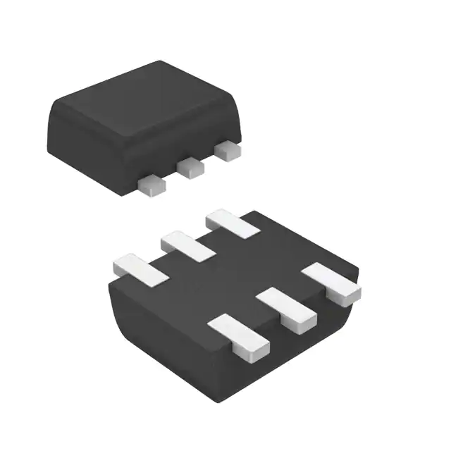
- Part No.:
- MMDT3904V-7
- Manufacturer:
- Diodes Incorporated
- Category:
- Bipolar Transistor Arrays
- Package:
- SOT-563, SOT-666
- Datasheet:
-
 MMDT3904V-7.pdf
- Description:
- TRANS 2NPN 40V 200MA SOT-563
- Quantity:
- Payment:

- Shipping:

Inventory:8,462
Please send an inquiry. Send us your inquiry, and we will respond immediately.
Product details
Overview
MMDT3904V-7 from Diodes Incorporated is a dual NPN small-signal transistor in SOT-563 package, designed for low-power amplification and switching functions. It features VCEO = 40 V, IC = 200 mA, PD = 200 mW, hFE = 40–300 (at IC = 100 µA to 100 mA), and fT = 300 MHz - enabling use in compact logic-level interface circuits and portable sensor signal conditioning.
For engineers reviewing the MMDT3904V-7 datasheet, MMDT3904V-7 pinout, MMDT3904V-7 application, or MMDT3904V-7 equivalent, key selection criteria include its dual-NPN configuration, SOT-563 footprint compatibility, low VCE(SAT) (0.20 V at IC = 10 mA), high fT, and RoHS-compliant green molding compound.
Technical Context
This dual NPN transistor uses epitaxial planar die construction for stable gain and low leakage. Its two independent NPN junctions share a common SOT-563 six-terminal package with isolated collectors and emitters, supporting discrete push-pull or differential pair topologies without cross-coupling.
Thermal performance is defined by RθJA = 625 °C/W on FR-4 PCB per AP02001 layout, and operation is rated from –55 °C to +150 °C. Switching parameters (td, tr, ts, tf) are specified under VCC = 3.0 V, enabling reliable 10–50 mA digital switching in space-constrained designs.
Key Specifications
| Parameter | Value and Actual Design Meaning |
|---|---|
| VCEO | 40 V - supports rail-to-rail switching up to 3.3 V/5 V logic systems with margin |
| IC (max) | 200 mA - sufficient for driving LEDs, small relays, or logic buffers |
| PD | 200 mW - limits continuous dissipation in unheatsinked SOT-563 layouts |
| hFE | 40–300 - enables bias stability across 0.1–100 mA collector loads |
| fT | 300 MHz - allows RF preamp or high-speed digital switching up to ~100 MHz |
| VCE(SAT) | 0.20 V @ IC=10 mA - minimizes voltage drop and power loss in saturated switch mode |
| NF | 5.0 dB @ IC=100 µA - suitable for low-noise audio or sensor front-end amplification |
Pinout & Package
Package: SOT-563 - ultra-small surface-mount plastic case (1.60 mm × 1.20 mm × 0.60 mm), UL 94V-0 rated, moisture sensitivity level 1.
| Pin/Terminal | Circuit Role | Design Meaning |
|---|---|---|
| 1 | Emitter of Transistor 1 | Low-impedance current sink node; tied to ground or reference in common-emitter switches |
| 2 | Base of Transistor 1 | Control input requiring ~0.7 V forward bias; drives with 1–5 mA for full saturation |
| 3 | Collector of Transistor 1 | Active output node; connects to load supply rail or pull-up resistor |
| 4 | Collector of Transistor 2 | Independent high-side output; electrically isolated from Q1 collector |
| 5 | Base of Transistor 2 | Second control input; identical drive requirements to Pin 2 |
| 6 | Emitter of Transistor 2 | Second independent emitter; may be tied separately or paralleled with Pin 1 |
Key Features
| Feature | Design Value |
|---|---|
| Dual isolated NPN structure | Enables compact differential pairs or independent switching channels in one footprint |
| Ultra-small SOT-563 package | Reduces board area by >40% vs. SO-8 or SC-70-6 equivalents |
| RoHS-compliant & "Green" molding compound | Meets global environmental compliance without halogen/Sb2O3 flame retardants |
| Low VCE(SAT) and high fT | Supports both efficient DC switching and mid-bandwidth analog amplification |
Applications
| Portable Sensor Interface | Logic-Level Translation |
|---|---|
Use Scenario: Amplifying weak analog outputs from MEMS accelerometers or temperature sensors in battery-powered wearables. IC Role / Device Role / Timing Role: Discrete NPN amplifier stage providing 20–50× voltage gain with <5 dB noise figure. Use Value: Enables direct ADC interfacing without external op-amps, reducing BOM count and quiescent current. | Use Scenario: Converting 1.8 V GPIO signals to 3.3 V levels for MCU peripherals in mixed-voltage IoT nodes. IC Role / Device Role / Timing Role: Active pull-up switch configured as level shifter with <35 ns rise/fall times. Use Value: Eliminates need for dedicated level-shifting ICs while maintaining timing integrity at 10 MHz data rates. |
| Dual-Channel LED Driver | Compact Push-Pull Output Stage |
Use Scenario: Driving two status LEDs (e.g., power + fault) from separate microcontroller pins in medical handheld devices. IC Role / Device Role / Timing Role: Two independent saturated switches controlling cathode-side LED current up to 20 mA each. Use Value: Saves PCB space versus two discrete SOT-23 transistors; shares thermal path and reduces assembly cost. | Use Scenario: Generating complementary square-wave outputs for gate driving or clock distribution in low-power FPGA I/O banks. IC Role / Device Role / Timing Role: Dual NPN pair configured as emitter-follower push-pull buffer with matched hFE tracking. Use Value: Improves drive strength and edge symmetry over single-transistor buffers, reducing EMI in 10–50 MHz clock paths. |
Equivalent & Alternatives
The following parts are listed as comparable options for similar dual NPN switching and amplification applications.
| Alternative Part | Technical Difference | Application Difference | Selection Advice |
|---|---|---|---|
| DMN3026LSD-13 | Single-channel N-channel MOSFET (30 V, 2.6 A); no bipolar gain or linear region | Better for high-current, low-VGS switching; unsuitable for analog amplification or low-IB drive | Select when replacing saturated-switch only functions with lower gate drive burden and higher ID |
| MMBT3904DW-7-F | Same die, identical specs, but in SOT-363 package (larger footprint, different pinout: 1–2–3 = E-B-C, 4–5–6 = C-B-E) | Requires PCB redesign; same electrical behavior and thermal derating | Choose only if legacy SOT-363 layout reuse is required; not drop-in compatible with SOT-563 |
Compared with DMN3026LSD-13 and MMBT3904DW-7-F, the MMDT3904V-7 uniquely delivers bipolar linearity, low-noise amplification capability, and minimal footprint - making it optimal where dual-channel analog gain or precise saturation control is needed within tight board area constraints.
Availability
MMDT3904V-7 is available at Aetrix Electronics and suitable for portable sensor interfaces, logic-level translation, dual-channel LED driving, and compact push-pull output stages requiring stable component supply and consistent green-material compliance.
Supply support for MMDT3904V-7 includes scheduled delivery planning, volume procurement assistance, BOM continuity management, traceable sourcing, and lifecycle availability coordination for OEM customers, industrial embedded developers, connected-device designers, and electronics production programs.
Manufacturer
Diodes Incorporated is a global manufacturer of discrete semiconductors and analog ICs, specializing in high-reliability, energy-efficient components for industrial, computing, and consumer markets.
The MMDT3904V-7 belongs to Diodes' small-signal transistor product line, engineered specifically for space-constrained, low-power amplification and switching applications where dual-device integration and environmental compliance are critical.
FAQ
What is the pin configuration for MMDT3904V-7 in SOT-563?
Pin 1 = Emitter of Q1, Pin 2 = Base of Q1, Pin 3 = Collector of Q1, Pin 4 = Collector of Q2, Pin 5 = Base of Q2, Pin 6 = Emitter of Q2. This arrangement supports independent operation of both transistors with shared thermal mass but no internal connection between channels.
Is MMDT3904V-7 suitable for linear amplification applications?
Yes - its hFE range (40–300), low NF (5.0 dB), and fT = 300 MHz support Class-A and Class-AB small-signal amplification up to ~50 MHz. Bias stability is confirmed across IC = 100 µA to 10 mA per the datasheet's Fig. 3 and Fig. 4.
How does the SOT-563 package affect thermal performance?
RθJA = 625 °C/W is measured on a standard FR-4 PCB per AP02001 layout. Derating begins above 25 °C ambient (Fig. 1), limiting usable PD to ~120 mW at 70 °C ambient - requiring careful layout or reduced IC in enclosed environments.
Does MMDT3904V-7 have qualified lead-free and halogen-free status?
Yes - it is lead-free by design and RoHS compliant (Note 3). Devices manufactured from Date Code UO (week 40, 2007) onward use green molding compound free of halogens and Sb2O3, verified per Diodes Inc.'s published Green Policy.
MMDT3904V-7 Specifications
- Product attributes
- Attribute value
- Manufacturer:
- Diodes Incorporated
- Series:
- -
- Package/Case:
- SOT-563, SOT-666
- Packaging:
- Tape & Reel (TR)
- Product Status:
- Obsolete
- Transistor Type:
- 2 NPN (Dual)
- Current - Collector (Ic) (Max):
- 200mA
- Voltage - Collector Emitter Breakdown (Max):
- 40V
- Vce Saturation (Max) @ Ib, Ic:
- 300mV @ 5mA, 50mA
- Current - Collector Cutoff (Max):
- -
- DC Current Gain (hFE) (Min) @ Ic, Vce:
- 100 @ 10mA, 1V
- Power - Max:
- 200mW
- Frequency - Transition:
- 300MHz
- Operating Temperature:
- -55°C ~ 150°C (TJ)
- Grade:
- -
- Qualification:
- -
- Mounting Type:
- Surface Mount
- Supplier Device Package:
- SOT-563
MMDT3904V-7 FAQ
1.How can I place an order for MMDT3904V-7 through Aetrix?
Please submit a Request for Quotation (RFQ) for MMDT3904V-7 on Aetrix. Our sales agent will provide a competitive quotation and guide you through the order confirmation once you accept the terms.
2.Are the price and stock information for MMDT3904V-7 reliable?
The price and inventory of MMDT3904V-7 are updated periodically and may fluctuate due to market conditions. Stock and pricing data are typically refreshed every 24 hours. Quotation validity for MMDT3904V-7 is usually 5 days.
3.What payment methods are accepted for MMDT3904V-7?
We accept Wire Transfer, PayPal, Credit Card, Western Union, MoneyGram, and Escrow for MMDT3904V-7 transactions.
Note: Certain payment methods may incur a processing fee.
4.How is shipping managed for MMDT3904V-7?
MMDT3904V-7 orders can be shipped via leading logistics carriers, including DHL, UPS, FedEx, TNT, or Registered Mail.
Once your MMDT3904V-7 order is processed, you will receive an email with the shipment details and tracking number.
Note: Tracking information may take up to 24 hours to appear. Express delivery typically takes 3–5 business days.
5.How can I obtain technical support or documentation for MMDT3904V-7?
For technical support, including MMDT3904V-7 datasheets, pinout diagrams, or application guidance, please contact our engineering support team. They can provide detailed documentation and assistance for your MMDT3904V-7 requirements.
6.How does Aetrix verify that MMDT3904V-7 is sourced from the original manufacturer or authorized distributors?
All MMDT3904V-7 products on Aetrix are procured from qualified distributors and authorized channels. Our dedicated quality assurance team conducts strict verification, including traceability checks and, if necessary, third-party testing. This ensures that MMDT3904V-7 meets industry standards.
7.What is the process for return or replacement of MMDT3904V-7?
All MMDT3904V-7 units undergo pre-shipment inspection (PSI). If there is an issue with MMDT3904V-7, returns or replacements are accepted under the following conditions:
1.Quantity discrepancies, incorrect items, or visible external defects (such as breakage or corrosion), acknowledged by Aetrix.
2.The issue is reported within 90 days of delivery.
3.The MMDT3904V-7 part is unused and in its original packaging.
Return procedure for MMDT3904V-7:
1.Submit a request within 90 days.
2.Obtain a Return Material Authorization (RMA) from Aetrix.
MMDT3904V-7 Tags

-
MBT3946DW1T1G
onsemi
-
BC846BPDW1T1G
onsemi
-
MBT2222ADW1T1G
onsemi
-
BC847BDW1T1G
onsemi

-
DMMT5401-7-F
Diodes Incorporated
-
DMMT5551-7-F
Diodes Incorporated
-
DMMT3904W-7-F
Diodes Incorporated
-
DMMT3906W-7-F
Diodes Incorporated
-
FMB3904
onsemi
-
FMB2222A
onsemi
-
ULQ2003D1013TR
STMicroelectronics
-
ZXTD4591E6TA
Diodes Incorporated
Tech Hub

An engineering guide to LED driver operation, constant-current and constant-voltage outputs, linear and switching topologies, dimming, IC selection, calculations, replacement compatibility, and fault c…

Operational amplifier guide covering op amp basics, feedback, ideal vs real op amps, common configurations, buffer circuits, offset, bias current, gain-bandwidth, slew rate, rail-to-rail limits and sel…

Jumper cables guide covering safe connection order, red and black clamp placement, final ground connection, cable gauge, length, clamp quality, copper vs CCA cables, jump starter comparison and battery…

LDO regulator guide covering low dropout voltage, power dissipation, thermal design, PSRR, output noise, capacitor stability, adjustable LDO circuits, LDO vs buck converter and datasheet selection chec…

Conditional Access Module guide covering CAM meaning, CI/CI+ interface, smart card authorization, DVB security workflow, TV and set-top box compatibility, internal electronics, ESD protection, connecto…

Guide to electronic component obsolescence covering EOL risk, PCN/PDN notices, last-time buy planning, replacement options, form-fit-function validation, counterfeit risk and BOM lifecycle management.

18650 battery guide covering lithium-ion cell basics, 3.6V/3.7V voltage, 4.2V charging, mAh and Wh capacity, protected cells, chargers, BMS, series-parallel packs, holders, welding and sourcing checks.…

Hall effect sensor guide covering working principle, linear and digital sensors, Arduino circuits, current sensing, speed detection, automotive applications, A3144 examples, signal filtering and datash…

Product Change Notification guide for electronic components, covering PCN meaning, PCN vs PDN/EOL, common change types, risk levels, form-fit-function review, engineering validation, BOM control, LTB/L…

A practical guide to blend door actuators, covering HVAC function, symptoms, location, AC and heater issues, reset and calibration, replacement cost, electrical diagnosis, compatibility checks, and rep…


