
 My Inquiry
 My Account


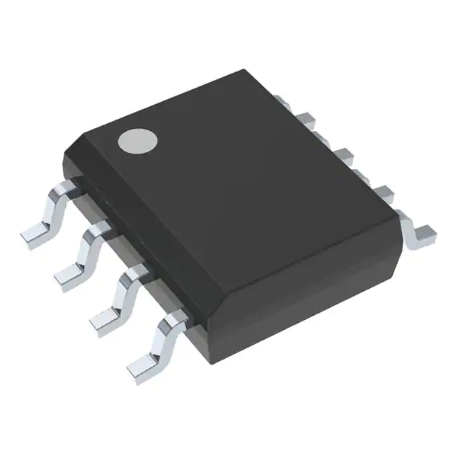
Monolithic Power Systems Inc. MP201DS-LF
- Part No.:
- MP201DS-LF
- Manufacturer:
- Monolithic Power Systems Inc.
- Category:
- Power Management - Specialized
- Package:
- 8-SOIC (0.154", 3.90mm Width)
- Datasheet:
-
 MP201DS-LF.pdf
- Description:
- IC REG LDO 42V 30MA
- Quantity:
- Payment:

- Shipping:

Inventory:3,950
Please send an inquiry. Send us your inquiry, and we will respond immediately.
Product details
Overview
MP201DS-LF from Monolithic Power Systems is a dying gasp storage and release control IC that manages energy backup during input power failure. It charges an external storage capacitor to a user-programmable voltage (up to 32 V) during normal operation, then dumps up to 2.5 A into the VIN rail when input voltage drops below a programmable release threshold (e.g., 10.2 V), sustaining regulated operation for critical communication handoff in DSL modems and home gateways.
For engineers reviewing the MP201DS-LF datasheet, MP201DS-LF pinout, MP201DS-LF application, or MP201DS-LF equivalent, this device requires attention to BST-SW node coupling, FB1/FB2 resistor selection for storage/release voltage setting, GASP open-drain signaling timing (73 µs rise delay), thermal derating at >125°C junction, and SOIC-8 layout constraints for STRG/VMAX decoupling.
Technical Context
The MP201DS-LF implements dual feedback regulation: FB1 monitors storage voltage (VSTRG) with 1.0 V ±3% reference and 50 mV hysteresis for refresh control; FB2 senses input voltage (VIN) with identical 1.0 V reference to trigger release when VIN falls below programmed threshold. Its internal boost/charge/release circuitry uses the BST pin-tied to a DC/DC converter's switch node-to generate gate drive for charging the storage capacitor.
During release, it regulates VIN near the release voltage by sinking current from STRG to VIN via an integrated power path capable of 2.5 A continuous dump current, while limiting pre-charge inrush to 260 mA. The GASP pin provides open-drain status indication synchronized to FB2 crossing 1.05×VFB2 (high) or 1.00×VFB2 (low), with 0.7 µs fall time and 4 mA sink capability at 0.3 V.
Key Specifications
| Parameter | Value and Actual Design Meaning |
|---|---|
| Input Voltage Range | 4.5 V to 18 V - supports wide-range telecom power rails including 12 V and 15 V DSL/PON systems |
| Storage Voltage Range | VIN to 2×VIN–0.8 V (max 32 V) - enables high-energy density storage using standard 25 V electrolytic capacitors |
| Dump Current Limit | 2.5 A typical - sustains ≥10 V output under 1 A load for ~20 ms with 2200 µF storage capacitance |
| Pre-charge Current Limit | 260 mA typical - prevents inrush damage during initial storage capacitor charge from 0 V to VIN |
| Feedback Reference Voltage | 1.0 V ±3% on FB1 and FB2 - sets precise storage/release thresholds via resistor dividers (e.g., R1=845 kΩ, R2=37.4 kΩ → VSTRG=23 V) |
| GASP Delay Times | Rising: 73 µs; Falling: 0.7 µs - ensures clean power-fail flag assertion before system shutdown |
| Thermal Shutdown | 150 °C with 30 °C hysteresis - protects against sustained overloads in enclosed gateway enclosures |
Pinout & Package
MP201DS-LF is housed in a standard SOIC-8 package (5.0 mm × 6.2 mm, 1.27 mm pitch) with exposed pad not present; JEDEC MS-012 compliant footprint and recommended land pattern provided in datasheet.
| Pin/Terminal | Circuit Role | Design Meaning |
|---|---|---|
| BST | Bootstrap driver output | Connects via RC network to DC/DC switch node to generate gate drive for storage capacitor charging; must be routed short and low-inductance |
| VIN | Main input supply rail | 4.5–18 V input source; requires local 47 µF ceramic + bulk capacitor; powers internal LDO (VMAX) |
| FB2 | Release voltage sense input | Resistor divider from VIN sets release threshold; triggers dump action when VIN < VFB2 × (1 + R3/R4) |
| GND | Analog/digital ground reference | Single-point star connection required; ties all internal references and feedback paths to system ground plane |
| FB1 | Storage voltage sense input | Resistor divider from STRG sets storage target; initiates refresh when VSTRG drops below VFB1 × (1 + R1/R2) |
| GASP | Open-drain power-fail indicator | Pulled low when VIN < VFB2; pulled high via external pull-up when VIN > 1.05×VFB2; used for MCU interrupt or status LED |
| STRG | Storage capacitor connection | High-current node for energy storage/release; connects directly to cathode of 25 V electrolytic capacitor (e.g., 2200 µF) |
| VMAX | Internal LDO supply | Requires 2.2 nF ceramic decoupling capacitor; powers internal logic and regulation circuitry independent of VIN ripple |
Key Features
| Feature | Design Value |
|---|---|
| User-programmable storage voltage | Set from VIN to 32 V via FB1 resistor divider - eliminates need for fixed-voltage storage ICs and enables optimal capacitor utilization |
| Controlled energy release | 2.5 A regulated dump current into VIN - maintains stable input rail during brownout, enabling graceful firmware save and network disconnect |
| Integrated pre-charge current limit | 260 mA soft-start for storage capacitor - avoids tripping upstream fuses or causing input rail sag during power-up |
| Dying gasp status signaling | GASP open-drain output with 73 µs rise/0.7 µs fall timing - provides deterministic MCU-triggered shutdown window before VIN collapse |
| Thermal protection with hysteresis | 150 °C shutdown + 30 °C recovery - prevents latch-up during transient overload or poor PCB heatsinking in compact gateways |
Applications
| Cable Modem Power Backup | DSL Access Point Hold-up |
|---|---|
Use Scenario: Residential cable modem loses upstream power but must maintain DOCSIS registration and send last heartbeat before shutdown. IC Role / Device Role / Timing Role: MP201DS-LF stores energy during normal operation and releases it to sustain VIN at 10.2 V for ≥15 ms after AC loss, powering RF front-end and PHY until graceful logout completes. Use Value: Enables compliance with FCC Part 15 hold-up requirements without oversized bulk capacitors or secondary battery circuits. | Use Scenario: DSLAM-facing access point experiences brief grid interruption; must retain VLAN configuration and avoid MAC table flush. IC Role / Device Role / Timing Role: Acts as intelligent hold-up controller: charges 2200 µF storage cap to 23 V, then dumps 2.5 A into VIN to extend regulated 12 V rail operation during 10–25 ms brownouts. Use Value: Reduces packet loss and session drop rate by extending functional uptime beyond standard 5–8 ms capacitor hold-up. |
| PON Optical Network Terminal | Home Gateway Power Sequencing |
Use Scenario: GPON ONT loses PSE power but must complete optical signal deactivation sequence and report fault to OLT before power depletion. IC Role / Device Role / Timing Role: MP201DS-LF monitors 12 V input; upon UVLO detection, asserts GASP and releases stored energy to maintain 10.2 V rail for 20+ ms, powering EPON MAC and laser driver shutdown logic. Use Value: Prevents unclean optical disconnection that could trigger false OLT alarms or require manual reset. | Use Scenario: Multi-band Wi-Fi 6 gateway with separate 3.3 V, 5 V, and 12 V rails must coordinate controlled shutdown across subsystems during AC loss. IC Role / Device Role / Timing Role: Provides centralized dying gasp timing signal (GASP) and rail stabilization, synchronizing PMIC sequencing and flash write completion across SoC, RAM, and radio ICs. Use Value: Eliminates data corruption risk during unexpected power loss by guaranteeing ≥18 ms of coordinated hold-up across all voltage domains. |
Equivalent & Alternatives
The following parts are listed as comparable options for similar dying gasp control applications.
| Alternative Part | Technical Difference | Application Difference | Selection Advice |
|---|---|---|---|
| TPS65235-1RGET | Integrated buck converter + dying gasp controller; 1.2 A max dump current; requires external storage FET | Designed for single-chip PoE-powered devices; lacks programmable storage voltage; smaller solution size but lower energy capacity | Select when space-constrained PoE endpoint design needs integrated DC/DC + hold-up, and 1.2 A dump current suffices |
| MAX16050ETA+ | Supervisory IC with programmable reset and power-fail comparator; no built-in charge/dump circuitry - requires external MOSFETs and gate drivers | Used in industrial PLCs where discrete power-path control and high reliability are prioritized over integration | Select when full design flexibility over storage topology and dump timing is required, and board area is not constrained |
Compared with TPS65235-1RGET and MAX16050ETA+, MP201DS-LF uniquely delivers standalone, high-current (2.5 A), fully programmable storage/release control in SOIC-8 - eliminating external FETs while supporting higher energy hold-up than integrated PMICs and avoiding complexity of discrete supervisory + power-path designs.
Availability
MP201DS-LF is available at Aetrix Electronics and suitable for cable modem power backup, DSL access point hold-up, and PON optical network terminal applications requiring stable component supply, RoHS-compliant packaging, and long-term lifecycle support.
Supply support for MP201DS-LF includes scheduled delivery planning, volume procurement assistance, BOM continuity management, traceable sourcing, and lifecycle availability coordination for OEM customers, industrial embedded developers, connected-device designers, and electronics production programs.
Manufacturer
Monolithic Power Systems (MPS) is a fabless semiconductor company specializing in high-performance analog and power ICs, with design centers in the US, China, and Taiwan, and global manufacturing partnerships.
The MP201 product line targets telecom infrastructure power management, specifically addressing the need for reliable, programmable dying gasp functionality in broadband access equipment without external power switches or complex control logic.
FAQ
What is the maximum storage voltage the MP201DS-LF can regulate?
The MP201DS-LF supports storage voltages from VIN up to 2×VIN – 0.8 V, with an absolute maximum rating of 32 V on the STRG pin. In practice, with 12 V input, it safely regulates storage to 23 V using the recommended R1/R2 divider (845 kΩ/37.4 kΩ), enabling use of standard 25 V electrolytic capacitors at 90% voltage derating.
How does the GASP pin behave during input voltage transition?
GASP is an open-drain output that pulls low when FB2 voltage falls below 1.00×VFB2 (i.e., VIN < release threshold), and releases to float when FB2 exceeds 1.05×VFB2. With a 10 kΩ pull-up to VIN, it transitions in 73 µs (rise) and 0.7 µs (fall), providing a clean, jitter-free power-fail flag for MCU interrupt service routines.
Can the MP201DS-LF operate without a DC/DC converter?
No - the BST pin requires connection to a switching node (SW) of an external DC/DC converter to generate the bootstrap voltage needed for storage capacitor charging. Without active switching, the MP201DS-LF cannot boost or regulate VSTRG above VIN; it only performs passive monitoring and release if pre-charged externally.
What is the purpose of the VMAX pin and its required capacitor?
VMAX supplies the internal LDO that powers MP201DS-LF's logic, comparators, and control circuitry independently of VIN ripple. A 2.2 nF ceramic capacitor between VMAX and GND is mandatory to stabilize this internal rail; omitting it causes erratic FB1/FB2 sampling and GASP glitches due to insufficient decoupling of the 260 µA quiescent supply.
How is storage capacitance calculated for a target hold-up time?
Required storage capacitance is calculated as CS = (IRELEASE × TDASP) / (VSTORAGE − VRELEASE). For example: 1 A release current, 20 ms hold-up, 23 V storage, and 10.2 V release yields CS = (1 × 0.02) / (23 − 10.2) ≈ 1560 µF. A 2200 µF/25 V electrolytic capacitor is recommended to account for aging and tolerance.
Does the MP201DS-LF support reverse current blocking during release?
Yes - during release mode, the internal power path is unidirectional: current flows only from STRG to VIN. The device incorporates body-diode blocking and active gate control to prevent reverse current from VIN back into the storage capacitor, ensuring energy is delivered solely to sustain the input rail and not wasted in leakage paths.
MP201DS-LF Specifications
- Product attributes
- Attribute value
- Manufacturer:
- Monolithic Power Systems Inc.
- Series:
- -
- Package/Case:
- 8-SOIC (0.154", 3.90mm Width)
- Packaging:
- Tube
- Product Status:
- Active
- Applications:
- Energy Storage Device
- Current - Supply:
- 250µA
- Voltage - Supply:
- 4.5V ~ 18V
- Operating Temperature:
- -40°C ~ 125°C
- Grade:
- -
- Qualification:
- -
- Mounting Type:
- Surface Mount
- Supplier Device Package:
- 8-SOIC
MP201DS-LF FAQ
1.How can I place an order for MP201DS-LF through Aetrix?
Please submit a Request for Quotation (RFQ) for MP201DS-LF on Aetrix. Our sales agent will provide a competitive quotation and guide you through the order confirmation once you accept the terms.
2.Are the price and stock information for MP201DS-LF reliable?
The price and inventory of MP201DS-LF are updated periodically and may fluctuate due to market conditions. Stock and pricing data are typically refreshed every 24 hours. Quotation validity for MP201DS-LF is usually 5 days.
3.What payment methods are accepted for MP201DS-LF?
We accept Wire Transfer, PayPal, Credit Card, Western Union, MoneyGram, and Escrow for MP201DS-LF transactions.
Note: Certain payment methods may incur a processing fee.
4.How is shipping managed for MP201DS-LF?
MP201DS-LF orders can be shipped via leading logistics carriers, including DHL, UPS, FedEx, TNT, or Registered Mail.
Once your MP201DS-LF order is processed, you will receive an email with the shipment details and tracking number.
Note: Tracking information may take up to 24 hours to appear. Express delivery typically takes 3–5 business days.
5.How can I obtain technical support or documentation for MP201DS-LF?
For technical support, including MP201DS-LF datasheets, pinout diagrams, or application guidance, please contact our engineering support team. They can provide detailed documentation and assistance for your MP201DS-LF requirements.
6.How does Aetrix verify that MP201DS-LF is sourced from the original manufacturer or authorized distributors?
All MP201DS-LF products on Aetrix are procured from qualified distributors and authorized channels. Our dedicated quality assurance team conducts strict verification, including traceability checks and, if necessary, third-party testing. This ensures that MP201DS-LF meets industry standards.
7.What is the process for return or replacement of MP201DS-LF?
All MP201DS-LF units undergo pre-shipment inspection (PSI). If there is an issue with MP201DS-LF, returns or replacements are accepted under the following conditions:
1.Quantity discrepancies, incorrect items, or visible external defects (such as breakage or corrosion), acknowledged by Aetrix.
2.The issue is reported within 90 days of delivery.
3.The MP201DS-LF part is unused and in its original packaging.
Return procedure for MP201DS-LF:
1.Submit a request within 90 days.
2.Obtain a Return Material Authorization (RMA) from Aetrix.
MP201DS-LF Tags

-
TPS2511DGNR
Texas Instruments

-
UTC2000/MG
Microchip Technology

-
TUSB320HAIRWBR
Texas Instruments

-
TPS61252DSGR
Texas Instruments

-
PI5USB30216CXUAEX
Diodes Incorporated

-
SN6501DBVR
Texas Instruments

-
CYPD3177-24LQXQT
Infineon Technologies
-
SN6501QDBVRQ1
Texas Instruments

-
STUSB1600AQTR
STMicroelectronics

-
SN6505BDBVR
Texas Instruments
-
SN6501DBVT
Texas Instruments

-
TPS65150PWPR
Texas Instruments
Tech Hub

Operational amplifier guide covering op amp basics, feedback, ideal vs real op amps, common configurations, buffer circuits, offset, bias current, gain-bandwidth, slew rate, rail-to-rail limits and sel…

Jumper cables guide covering safe connection order, red and black clamp placement, final ground connection, cable gauge, length, clamp quality, copper vs CCA cables, jump starter comparison and battery…

LDO regulator guide covering low dropout voltage, power dissipation, thermal design, PSRR, output noise, capacitor stability, adjustable LDO circuits, LDO vs buck converter and datasheet selection chec…

Conditional Access Module guide covering CAM meaning, CI/CI+ interface, smart card authorization, DVB security workflow, TV and set-top box compatibility, internal electronics, ESD protection, connecto…

Guide to electronic component obsolescence covering EOL risk, PCN/PDN notices, last-time buy planning, replacement options, form-fit-function validation, counterfeit risk and BOM lifecycle management.

18650 battery guide covering lithium-ion cell basics, 3.6V/3.7V voltage, 4.2V charging, mAh and Wh capacity, protected cells, chargers, BMS, series-parallel packs, holders, welding and sourcing checks.…

Hall effect sensor guide covering working principle, linear and digital sensors, Arduino circuits, current sensing, speed detection, automotive applications, A3144 examples, signal filtering and datash…

Product Change Notification guide for electronic components, covering PCN meaning, PCN vs PDN/EOL, common change types, risk levels, form-fit-function review, engineering validation, BOM control, LTB/L…

A practical guide to blend door actuators, covering HVAC function, symptoms, location, AC and heater issues, reset and calibration, replacement cost, electrical diagnosis, compatibility checks, and rep…

Engineering guide to Raspberry Pi alternatives, covering chip-level differences, Orange Pi, ROCK, Jetson, Banana Pi, NanoPi, Compute Module, Pico, GPIO, camera, HAT compatibility, and replacement risks…


