
 My Inquiry
 My Account


Monolithic Power Systems Inc. MP2733GQC-0001-P
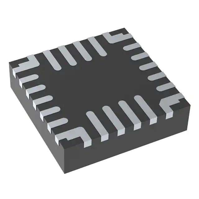
- Part No.:
- MP2733GQC-0001-P
- Manufacturer:
- Monolithic Power Systems Inc.
- Category:
- Power Management - Specialized
- Package:
- 26-PowerVFQFN
- Datasheet:
-
 MP2733GQC-0001-P.pdf
- Description:
- WIDE INPUT RANGE, 4.5A, I2C-CONT
- Quantity:
- Payment:

- Shipping:

Inventory:900
Please send an inquiry. Send us your inquiry, and we will respond immediately.
Product details
Overview
MP2733GQC-0001-P from Monolithic Power Systems is a 4.5A, I²C-controlled switch-mode battery charger IC for single-cell Li-ion/Li-polymer batteries, featuring NVDC power path management, USB OTG boost (up to 3A at 5V), integrated 8-bit ADC, and JEITA-compliant temperature monitoring. It operates from 3.7V–16V input, delivers 92% charge efficiency at 3A, and supports instant-on operation with deeply discharged or absent batteries - deployed in smartphones, tablets, and wireless cameras.
For engineers reviewing the MP2733GQC-0001-P datasheet, MP2733GQC-0001-P pinout, MP2733GQC-0001-P application, or MP2733GQC-0001-P equivalent, key selection considerations include its QFN-26 (3.5mm×3.5mm) package, 14mΩ BATTFET, 1.35MHz buck switching frequency, I²C-configurable charge voltage (3.4V–4.67V), and dual-role USB DP/DM interface for fast-charge protocol detection and OTG control.
Technical Context
The MP2733 implements a synchronous buck topology with fully integrated high-side (25mΩ) and low-side (25mΩ) MOSFETs, reverse-blocking FET (20mΩ), and BATTFET (14mΩ), enabling efficient charging and system power path arbitration. Its NVDC architecture decouples battery and system rails, allowing SYS to remain powered during battery charging or absence.
USB OTG is implemented via an internal boost converter controlled by I²C registers and the OTG pin, delivering 4.8V–5.5V output with up to 3A current limit. The integrated 8-bit ADC monitors six analog signals - VIN, IIN, VBATT, ICHG, VSYS, and NTC voltage - with ±2 LSB accuracy and configurable sampling.
Key Specifications
| Parameter | Value and Actual Design Meaning |
|---|---|
| Input Voltage Range | 3.7V to 16V - supports USB hosts, wall adapters, and fast-charge sources without external regulation. |
| Charge Current | Up to 4.5A - programmable via I²C (320mA–4520mA in 17.5mA steps) with ±3 LSB accuracy at 1.84A. |
| Battery Regulation | 3.4V to 4.67V - I²C-configurable with ±0.5% accuracy at 4.2V, supporting multiple Li-ion chemistries. |
| Switching Frequency | 1.35MHz (typ) - enables compact 1.0µH inductor and reduces EMI in space-constrained portable designs. |
| BATTFET RDS(on) | 14mΩ - minimizes discharge loss and supports up to 8.5A continuous battery discharge for high-power SYS loads. |
| ADC Resolution | 8-bit - measures VIN, VBATT, ICHG, VSYS, IIN, and VNTC with dedicated LSB values (e.g., 60mV for VIN, 20mV for VBATT). |
| USB OTG Output | 4.8V–5.5V adjustable, up to 3A - I²C- and pin-controlled boost mode with 93% efficiency at 1.5A output. |
| Shipping Mode Leakage | 13µA - achieved via DISC pin control and BATTFET disable, extending shelf life of pre-shipped devices. |
Pinout & Package
MP2733GQC-0001-P is housed in a thermally enhanced QFN-26 package (3.5mm × 3.5mm, 0.5mm pitch) with exposed thermal pad. Pin numbering follows standard top-view orientation per MPS datasheet Rev. 1.1.
| Pin/Terminal | Circuit Role | Design Meaning |
|---|---|---|
| 1, 26 (DP) | USB D+ data line | Configurable I/O for USB detection, fast-charge negotiation (BC1.2, DCP, CDP), and OTG host signaling. |
| 2 (IN) | Main power input | Accepts 3.7V–16V input; connects to 1µF ceramic bypass capacitor for noise suppression and transient response. |
| 3 (PMID) | Internal power rail | Drain node of reverse-blocking FET and HS-FET; requires 10µF local bypass to stabilize gate drive and reduce ripple. |
| 4 (SW) | Switching node | Connects to inductor and BST capacitor; critical for buck converter operation and EMI layout integrity. |
| 5–7 (PGND) | Power ground | Low-impedance return path for high-current switching loops; must be tied directly to thermal pad and external GND plane. |
| 8 (BST) | Bootstrap supply | Forms floating gate drive for HS-FET via 47nF capacitor to SW; enables 100% duty cycle capability. |
| 9 (STAT) | Open-drain status indicator | Signals charge state (trickle/pre-charge/CC/CV/complete/fault) with external 10kΩ pull-up to VREF. |
| 10 (INT) | Open-drain interrupt | Asserts on fault events (OVP, OCP, thermal shutdown, JEITA violation) for host processor notification. |
| 11 (NTC) | Temperature sense input | Analog input for NTC thermistor divider; used with VNTC to implement JEITA-compliant hot/cold/warm thresholds. |
| 12 (VNTC) | NTC bias reference | Provides stable 1.2V reference (derived from VREF) for NTC comparator; sets temperature window boundaries. |
| 13–14 (VREF) | Internal LDO output | 3.6V, 40mA LDO powering internal circuitry and external bias networks; requires 10µF ceramic decoupling. |
| 15 (AGND) | Analog ground | Separate ground for ADC, comparators, and reference circuits; must be star-connected to PGND at single point. |
| 16 (SYS) | System power output | Regulated system rail (VBATT-tracking or fixed); supplies SoC, display, and peripherals with ideal diode support. |
| 17 (BATT) | Battery positive terminal | Direct connection to single-cell Li-ion pack; bypassed with 22µF ceramic capacitor for low-ESR filtering. |
| 18 (CE) | Charge enable (active-low) | Hardware override for I²C-controlled charge enable/disable; low = charge enabled if register permits. |
| 19–20 (SCL) | I²C clock input | Standard-mode (100kHz) or fast-mode (400kHz) clock; requires 10kΩ pull-up to logic rail (1.8V/3.3V). |
| 21 (SDA) | I²C bidirectional data | Open-drain I/O; shares same 10kΩ pull-up as SCL; supports read/write of 48 registers including OTP map. |
| 22 (DISC) | Disconnection control | Enables shipping mode (BATTFET off, 13µA leakage) and system reset; debounced via I²C register REG0Ah. |
| 23 (OTG) | OTG boost enable | Hardware suspend control for boost mode; low = disables OTG output while preserving I²C configuration. |
| 24 (ILIM) | Input current limit set | Analog pin setting max input current (400mA–3A) via resistor-to-ground; overrides I²C value if lower. |
| 25 (DM) | USB D− data line | Complementary to DP; enables USB enumeration, BC1.2 detection, and OTG host negotiation. |
Key Features
| Feature | Design Value |
|---|---|
| NVDC Power Path Management | Enables instant-on system startup with no battery or deep discharge; maintains SYS voltage independent of battery state. |
| Integrated 8-Bit ADC | Monitors VIN, IIN, VBATT, ICHG, VSYS, and VNTC with ±2 LSB accuracy - eliminates need for external sensing ICs. |
| JEITA Temperature Compliance | Configurable hot/cold/warm thresholds (e.g., VHOT = 36.3% of VNTC) with hysteresis - ensures safe charging across ambient conditions. |
| Dedicated DISC Pin Control | Hardware-triggered shipping mode (13µA IBATT) and system reset - simplifies factory programming and field recovery. |
| USB Type Detection & Fast-Charge Support | D+/D− pins detect SDP/CDP/DCP and negotiate proprietary protocols (e.g., QC, AFC) without host CPU intervention. |
| Thermal Regulation & Watchdog | 112°C thermal foldback + 150°C shutdown; I²C watchdog (160s timeout) prevents firmware lockup-induced safety failures. |
Applications
| Smartphones | Tablet PCs |
|---|---|
|
Use Scenario: Compact form factor requiring simultaneous fast charging, system power delivery, and battery health monitoring under variable input sources (USB-C PD, wall adapter, wireless). IC Role / Device Role / Timing Role: Primary battery management IC handling charge control, NVDC path arbitration, USB OTG host emulation, and real-time battery telemetry via ADC. Use Value: Enables 4.5A charging with <92% efficiency, extends battery cycle life via JEITA compliance, and supports instant-on UX even with 0% battery. |
Use Scenario: High-power portable computing device needing robust power path management during concurrent charging, display backlight, and compute load. IC Role / Device Role / Timing Role: System power manager providing SYS rail regulation, battery supplement mode, and seamless transition between AC adapter and battery power. Use Value: Delivers up to 8.5A battery discharge through 14mΩ BATTFET, reducing voltage drop and thermal stress during peak SYS loads. |
| Wireless Cameras | Portable Medical Monitors |
|
Use Scenario: Battery-powered imaging device operating in outdoor environments with wide temperature swings and intermittent solar or USB input. IC Role / Device Role / Timing Role: Intelligent charger with NTC-based JEITA profiling, input source detection (solar MPPT-ready variant MP2733GQC-0001), and low-quiescent shipping mode. Use Value: Prevents charging outside safe thermal windows (e.g., suspends at >45°C), and maintains <16µA battery leakage in storage - preserving shelf life. |
Use Scenario: Life-critical handheld diagnostic tool requiring fail-safe battery operation, precise voltage/current monitoring, and regulatory-compliant thermal protection. IC Role / Device Role / Timing Role: Safety-certified power controller performing redundant battery voltage validation, over-voltage/over-current fault detection, and watchdog-monitored I²C communication. Use Value: Integrates battery OVP (103.5% of VBATT_REG), safety timer, and thermal shutdown - meeting IEC 62368-1 and UL 62368-1 requirements. |
Equivalent & Alternatives
The following parts are listed as comparable options for similar switch-mode battery charger applications.
| Alternative Part | Technical Difference | Application Difference | Selection Advice |
|---|---|---|---|
| BQ25618RTWR (TI) | 3A max charge current; 1.2MHz switching; no integrated USB DP/DM detection; separate NTC bias required. | Lacks native USB type detection and fast-charge negotiation - requires external BC1.2 IC or MCU firmware handling. | Select when lower cost and simpler USB integration are prioritized over 4.5A capacity and autonomous protocol detection. |
| ISL9241IRZ-T7A (Renesas) | 4.5A charge current; 1.2MHz; integrated ADC but only 6-bit resolution; no shipping mode DISC pin function. | Higher ADC quantization error (±4 LSB vs. ±2 LSB) limits precision telemetry; lacks hardware shipping mode control. | Choose when existing Renesas ecosystem and dual-battery support outweigh need for ultra-low shipping leakage and JEITA configurability. |
Compared with BQ25618RTWR and ISL9241IRZ-T7A, MP2733GQC-0001-P uniquely combines 4.5A charging, full USB DP/DM detection, 8-bit ADC telemetry, and dedicated DISC pin for certified shipping mode - making it optimal for premium portable devices demanding autonomous, safe, and high-efficiency power management.
Availability
MP2733GQC-0001-P is available at Aetrix Electronics and suitable for smartphones, tablets, and wireless cameras requiring stable component supply, long-term lifecycle support, and RoHS-compliant packaging.
Supply support for MP2733GQC-0001-P includes scheduled delivery planning, volume procurement assistance, BOM continuity management, traceable sourcing, and lifecycle availability coordination for OEM customers, industrial embedded developers, connected-device designers, and electronics production programs.
Manufacturer
Monolithic Power Systems (MPS) is a fabless semiconductor company specializing in high-performance power management ICs for consumer, industrial, and automotive markets.
The MP2733 belongs to MPS's advanced battery charger product line, designed specifically for high-efficiency, software-configurable, and safety-certifiable power management in space-constrained portable electronics.
FAQ
What input voltage range does MP2733GQC-0001-P support, and how does it handle overvoltage?
MP2733GQC-0001-P supports 3.7V to 16V input with sustained 22V absolute maximum rating. Input overvoltage protection triggers at 5.8V–6.3V (for 5V sources) or 16.2V–17.2V (for >5V sources), with 380mV hysteresis. This dual-threshold OVP prevents damage from transient surges or misconnected adapters while maintaining compatibility with USB PD and high-voltage wall chargers.
How does the NVDC power path enable instant-on functionality with a dead battery?
NVDC separates the system (SYS) rail from the battery (BATT) rail using internal ideal diode control. When the battery is absent or deeply discharged (<2.6V), SYS is powered directly from IN via the BATTFET in supplement mode, enabling immediate system boot. The 20mV forward voltage drop and automatic entry/exit hysteresis ensure seamless transitions without brownouts.
Can MP2733GQC-0001-P operate in shipping mode, and what is the battery leakage current?
Yes - asserting the DISC pin low (or configuring REG0Ah) disables the BATTFET and places the IC in shipping mode, reducing battery leakage to 13µA typical at 4.2V. This is achieved via internal bias shutdown and gate isolation, extending shelf life beyond 12 months without requiring external switches or PCB modifications.
What level of USB fast-charge protocol support does MP2733GQC-0001-P provide natively?
MP2733GQC-0001-P natively detects USB BC1.2 SDP/CDP/DCP and supports proprietary fast-charge negotiation via configurable D+/D− voltage thresholds (1.7V, 2.2V, 2.4V, 2.9V). It does not implement QC/AFC/PD PHY layers but provides the analog foundation for MCU-based protocol handshaking - eliminating need for discrete BC1.2 ICs.
How accurate is the integrated ADC, and which parameters does it measure?
The 8-bit ADC measures six parameters: VIN (±2 LSB, 60mV LSB), VBATT (±2 LSB, 20mV LSB), ICHG (±3 LSB, 17.5mA LSB), VSYS (±2 LSB, 20mV LSB), IIN (±4 LSB, 13.3mA LSB), and VNTC (±2 LSB, 0.392% LSB). All conversions occur internally without host polling overhead, enabling real-time telemetry for battery health algorithms.
Does MP2733GQC-0001-P require external MOSFETs, and what is its thermal performance?
No external MOSFETs are required - MP2733GQC-0001-P integrates all power switches: 20mΩ reverse-blocking FET, 25mΩ HS-FET, 25mΩ LS-FET, and 14mΩ BATTFET. With θJA = 48°C/W on a 4-layer board, it sustains 4.5A charging at TA = 25°C without thermal derating; junction temperature remains below 112°C under full load before regulation engages.
What safety protections are implemented, and how are faults reported?
Protections include input/system OVP, battery OVP (103.5% of VBATT_REG), thermal regulation (112°C) and shutdown (150°C), JEITA temperature windows, charging safety timer, and watchdog-monitored I²C. Faults assert the open-drain INT pin, and status is readable via I²C register REG0Bh - enabling host-driven recovery without hard reset.
MP2733GQC-0001-P Specifications
- Product attributes
- Attribute value
- Manufacturer:
- Monolithic Power Systems Inc.
- Series:
- -
- Package/Case:
- 26-PowerVFQFN
- Packaging:
- Tape & Reel (TR)
- Product Status:
- Active
- Applications:
- Battery Management, SmartPhones
- Current - Supply:
- 4mA
- Voltage - Supply:
- 3.7V ~ 16V
- Operating Temperature:
- -40°C ~ 125°C (TJ)
- Grade:
- -
- Qualification:
- -
- Mounting Type:
- Surface Mount
- Supplier Device Package:
- 26-QFN (3.5x3.5)
MP2733GQC-0001-P FAQ
1.How can I place an order for MP2733GQC-0001-P through Aetrix?
Please submit a Request for Quotation (RFQ) for MP2733GQC-0001-P on Aetrix. Our sales agent will provide a competitive quotation and guide you through the order confirmation once you accept the terms.
2.Are the price and stock information for MP2733GQC-0001-P reliable?
The price and inventory of MP2733GQC-0001-P are updated periodically and may fluctuate due to market conditions. Stock and pricing data are typically refreshed every 24 hours. Quotation validity for MP2733GQC-0001-P is usually 5 days.
3.What payment methods are accepted for MP2733GQC-0001-P?
We accept Wire Transfer, PayPal, Credit Card, Western Union, MoneyGram, and Escrow for MP2733GQC-0001-P transactions.
Note: Certain payment methods may incur a processing fee.
4.How is shipping managed for MP2733GQC-0001-P?
MP2733GQC-0001-P orders can be shipped via leading logistics carriers, including DHL, UPS, FedEx, TNT, or Registered Mail.
Once your MP2733GQC-0001-P order is processed, you will receive an email with the shipment details and tracking number.
Note: Tracking information may take up to 24 hours to appear. Express delivery typically takes 3–5 business days.
5.How can I obtain technical support or documentation for MP2733GQC-0001-P?
For technical support, including MP2733GQC-0001-P datasheets, pinout diagrams, or application guidance, please contact our engineering support team. They can provide detailed documentation and assistance for your MP2733GQC-0001-P requirements.
6.How does Aetrix verify that MP2733GQC-0001-P is sourced from the original manufacturer or authorized distributors?
All MP2733GQC-0001-P products on Aetrix are procured from qualified distributors and authorized channels. Our dedicated quality assurance team conducts strict verification, including traceability checks and, if necessary, third-party testing. This ensures that MP2733GQC-0001-P meets industry standards.
7.What is the process for return or replacement of MP2733GQC-0001-P?
All MP2733GQC-0001-P units undergo pre-shipment inspection (PSI). If there is an issue with MP2733GQC-0001-P, returns or replacements are accepted under the following conditions:
1.Quantity discrepancies, incorrect items, or visible external defects (such as breakage or corrosion), acknowledged by Aetrix.
2.The issue is reported within 90 days of delivery.
3.The MP2733GQC-0001-P part is unused and in its original packaging.
Return procedure for MP2733GQC-0001-P:
1.Submit a request within 90 days.
2.Obtain a Return Material Authorization (RMA) from Aetrix.
MP2733GQC-0001-P Tags

-
TPS2511DGNR
Texas Instruments

-
UTC2000/MG
Microchip Technology

-
TUSB320HAIRWBR
Texas Instruments

-
TPS61252DSGR
Texas Instruments

-
PI5USB30216CXUAEX
Diodes Incorporated

-
SN6501DBVR
Texas Instruments

-
CYPD3177-24LQXQT
Infineon Technologies
-
SN6501QDBVRQ1
Texas Instruments

-
STUSB1600AQTR
STMicroelectronics

-
SN6505BDBVR
Texas Instruments
-
SN6501DBVT
Texas Instruments

-
TPS65150PWPR
Texas Instruments
Tech Hub

Operational amplifier guide covering op amp basics, feedback, ideal vs real op amps, common configurations, buffer circuits, offset, bias current, gain-bandwidth, slew rate, rail-to-rail limits and sel…

Jumper cables guide covering safe connection order, red and black clamp placement, final ground connection, cable gauge, length, clamp quality, copper vs CCA cables, jump starter comparison and battery…

LDO regulator guide covering low dropout voltage, power dissipation, thermal design, PSRR, output noise, capacitor stability, adjustable LDO circuits, LDO vs buck converter and datasheet selection chec…

Conditional Access Module guide covering CAM meaning, CI/CI+ interface, smart card authorization, DVB security workflow, TV and set-top box compatibility, internal electronics, ESD protection, connecto…

Guide to electronic component obsolescence covering EOL risk, PCN/PDN notices, last-time buy planning, replacement options, form-fit-function validation, counterfeit risk and BOM lifecycle management.

18650 battery guide covering lithium-ion cell basics, 3.6V/3.7V voltage, 4.2V charging, mAh and Wh capacity, protected cells, chargers, BMS, series-parallel packs, holders, welding and sourcing checks.…

Hall effect sensor guide covering working principle, linear and digital sensors, Arduino circuits, current sensing, speed detection, automotive applications, A3144 examples, signal filtering and datash…

Product Change Notification guide for electronic components, covering PCN meaning, PCN vs PDN/EOL, common change types, risk levels, form-fit-function review, engineering validation, BOM control, LTB/L…

A practical guide to blend door actuators, covering HVAC function, symptoms, location, AC and heater issues, reset and calibration, replacement cost, electrical diagnosis, compatibility checks, and rep…

Engineering guide to Raspberry Pi alternatives, covering chip-level differences, Orange Pi, ROCK, Jetson, Banana Pi, NanoPi, Compute Module, Pico, GPIO, camera, HAT compatibility, and replacement risks…


