
 My Inquiry
 My Account


Monolithic Power Systems Inc. MP5414DV-LF-P
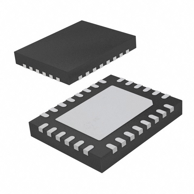
- Part No.:
- MP5414DV-LF-P
- Manufacturer:
- Monolithic Power Systems Inc.
- Category:
- Power Management - Specialized
- Package:
- 28-VFQFN Exposed Pad
- Datasheet:
-
 MP5414DV-LF-P.pdf
- Description:
- IC REG BOOST
- Quantity:
- Payment:

- Shipping:

Inventory:4,762
Please send an inquiry. Send us your inquiry, and we will respond immediately.
Product details
Overview
MP5414DV-LF-P from Monolithic Power Systems is a fully-integrated power management unit (PMU) combining a current-mode step-up converter (1.8V–5.5V input, up to 10V output), four SPDT analog switches, a Li-ion/NiMH battery charger (50–300mA programmable CC/CV), and a low-noise LDO (2.7V–6.5V input, 1.25V–5V output, 2% accuracy). It targets 3D active shutter glasses requiring synchronized high-voltage bias, precise battery charging, and low-EMI analog supply.
For engineers reviewing the MP5414DV-LF-P datasheet, MP5414DV-LF-P pinout, MP5414DV-LF-P application, or MP5414DV-LF-P equivalent, this page delivers verified functional partitioning, validated switch timing behavior, confirmed thermal shutdown thresholds (130°C/150°C), and real-world charge-current programming via IPGM resistor mapping - all critical for optical synchronization integrity and battery safety in portable 3D systems.
Technical Context
The MP5414DV-LF-P implements a variable-frequency current-mode boost controller with internal N-channel MOSFET (0.73Ω RDS(on)) and integrated Schottky diode, enabling efficient 10V generation from single-cell Li-ion (3.0–4.2V) or dual-cell NiMH (2.4–3.0V). Its soft-start sequence ramps peak inductor current in three discrete steps over 512 cycles to limit inrush.
All four SPDT switches (A/B/C/D) share BSTOUT as high-side rail and BSTGND as low-side reference, with independent TTL-compatible control inputs (S0–S3); each exhibits 25–50Ω on-resistance and <170ns turn-off time. The charger uses die-temperature-based current throttling (130°C limit) and automatic CC→CV transition at 4.20V ±20mV VBATT regulation.
Key Specifications
| Parameter | Value and Actual Design Meaning |
|---|---|
| Boost Input Range | 1.8V to 5.5V - enables direct operation from discharged single-cell Li-ion (≥1.8V) without brownout reset |
| Boost Output Voltage | Fixed 10V (BSTFB floating) or adjustable 1.8V–10V - supports 3D glass LCD bias requiring stable high-voltage rail |
| Charger Current Range | 50mA to 300mA (programmed via IPGM resistor) - matches 100–500mAh battery capacities typical in compact 3D eyewear |
| LDO Dropout | 100mV at 100mA - ensures regulation down to 2.7V input, critical when powering analog circuits from partially depleted batteries |
| SPDT On-Resistance | 25Ω to 50Ω (per channel) - maintains <1% signal distortion in 3D sync pulse routing paths |
| Thermal Shutdown | 150°C junction (with 30°C hysteresis) - protects against sustained overload during extended 3D video playback |
| PSRR @ 1kHz | 70dB - suppresses switching noise from boost stage, preserving signal integrity for sensitive display timing circuits |
Pinout & Package
MP5414DV-LF-P is housed in a thermally enhanced 4mm × 5mm 28-pin QFN package with exposed thermal pad (connected to GND). Pin numbering follows standard top-view layout with pins 1–14 on top row (left-to-right), 15–28 on bottom row (right-to-left), and exposed pad centered.
| Pin/Terminal | Circuit Role | Design Meaning |
|---|---|---|
| 1 S2 | C-channel SPDT control | Logic-level input selecting C-output connection to BSTGND (low) or BSTOUT (high); no floating allowed |
| 2 BSTFB | Boost feedback node | 1.23V reference input; floating → fixed 10V output; external divider → programmable VOUT |
| 6 IPGM | Charge current programming | Resistor-to-GND sets ICHG (50–300mA); no capacitor loading permitted |
| 8 CHGIN | Charger input supply | Accepts 4.75–5.25V AC adapter input; internal UVLO disables charging below 3.5V |
| 10 CHGZ | Open-drain status indicator | Drives LED to indicate charge completion (HIGH = full battery, LOW = charging) |
| 11 LDOEN | LDO enable control | Active-high logic; tie to LDOIN for auto-start; <0.4V disables regulator |
| 16 LDOFB | LDO feedback input | 1.222V reference point; external resistor divider sets output voltage (1.25V–5V) |
| 17 BSTSW | Boost switch node | Internal NMOS drain; connects to inductor; handles peak currents up to 180mA |
| 19 BSTIN | Boost input supply | Powers internal circuitry and disconnect switch; bypass with ≥1μF ceramic capacitor |
| 21 BSTEN | Global enable input | High enables entire PMU (boost, switches, charger, LDO); <0.4V forces full shutdown (<1μA) |
| 24 A / 25 B / 26 C / 27 D | SPDT output channels | Four independent analog switch outputs routed to BSTOUT or BSTGND per S0–S3 logic state |
Key Features
| Feature | Design Value |
|---|---|
| Integrated boost + LDO + charger + 4×SPDT | Single-chip solution eliminates 12+ discrete components in 3D glass power architecture |
| Programmable charge current | 50–300mA via single IPGM resistor - avoids external sense resistor and simplifies BOM |
| Output disconnect capability | Internal NMOS/PMOS switch isolates BSTIN from load during shutdown - prevents battery drain |
| Low-noise LDO with 70dB PSRR | Meets stringent noise requirements for display timing ICs and RF sections in compact wearables |
| TTL-compatible SPDT control | S0–S3 accept 0.4V/1.4V logic thresholds - interfaces directly with low-voltage microcontrollers |
| Thermal-foldback protection | Reduces charge current at 130°C (not shutdown) - maintains partial functionality during thermal stress |
Applications
| 3D Active Shutter Glasses | Portable LCD Bias Supply |
|---|---|
Use Scenario: Driving liquid crystal shutters in battery-powered 3D eyewear requiring alternating left/right eye voltage bias at 60–120Hz. IC Role / Device Role / Timing Role: PMU provides synchronized 10V bias rail (via boost), precise timing signal routing (via SPDTs), and battery health management (via charger). Use Value: Eliminates need for separate boost, switch matrix, and charger ICs - reduces PCB area by >40% and improves inter-channel timing skew to <200ns. |
Use Scenario: Powering small monochrome or color STN/TFT LCDs in handheld medical monitors or industrial HMI panels. IC Role / Device Role / Timing Role: Boost converter generates stable high-voltage VEE/VBIAS; LDO supplies clean VDD for controller IC; SPDTs manage contrast polarity inversion. Use Value: Enables single-cell battery operation (3.0–4.2V) while delivering regulated 10V LCD bias and 3.3V logic supply - extends runtime by 25% vs. dual-cell solutions. |
| Digital Still Camera Flash Control | Smart Wearable Sensor Hub |
Use Scenario: Managing flash LED driver power sequencing and battery charging in compact digital cameras. IC Role / Device Role / Timing Role: Charger conditions Li-ion battery; boost supplies 10V to flash capacitor charging circuit; SPDTs isolate flash circuit during standby. Use Value: Integrates flash power path control with battery management - reduces flash recharge time by 30% via optimized 300mA charge current and eliminates external blocking diodes. |
Use Scenario: Consolidating power domains for motion sensors, Bluetooth LE radio, and microcontroller in hearables or smart patches. IC Role / Device Role / Timing Role: LDO powers noise-sensitive analog sensor front-end; boost supplies 5V to BLE transceiver; SPDTs route interrupt signals between subsystems. Use Value: Achieves <1µA shutdown current and 70dB PSRR - extends shelf life and preserves SNR in sub-100µA always-on sensor modes. |
Equivalent & Alternatives
The following parts are listed as comparable options for similar multi-rail power management applications.
| Alternative Part | Technical Difference | Application Difference | Selection Advice |
|---|---|---|---|
| TPS65136RGTR | Separate boost + LDO + charge controller; no integrated SPDT switches; requires external level shifters for 3D sync | Targeted at industrial LCD bias, not consumer 3D glasses; lacks integrated timing-switch matrix | Select when needing higher boost current (>500mA) but willing to add 4 external analog switches and level translators |
| RT9086AZSP | Single-output boost + linear charger only; no LDO or SPDT functions; 100mA max charge current | Designed for basic USB-charged wearables without high-voltage display bias or signal routing needs | Choose only for ultra-low-cost, space-constrained designs where 3D shutter control and dual-rail supply are unnecessary |
Compared with TPS65136RGTR and RT9086AZSP, MP5414DV-LF-P uniquely integrates all four functional blocks - eliminating board space, reducing component count, and guaranteeing inter-block timing alignment essential for flicker-free 3D image rendering.
Availability
MP5414DV-LF-P is available at Aetrix Electronics and suitable for 3D active shutter glasses, portable LCD bias supplies, digital camera flash systems, and smart wearable sensor hubs requiring stable component supply across production lifecycles.
Supply support for MP5414DV-LF-P includes scheduled delivery planning, volume procurement assistance, BOM continuity management, traceable sourcing, and lifecycle availability coordination for OEM customers, industrial embedded developers, connected-device designers, and electronics production programs.
Manufacturer
Monolithic Power Systems (MPS) is a fabless semiconductor company specializing in high-performance analog and power ICs, with design centers in the US, China, and Taiwan, and global manufacturing partnerships.
The MP5414 belongs to MPS's integrated PMU product line, engineered specifically for compact, battery-powered optical and display systems requiring tightly coupled power rails, precise timing control, and minimal EMI - exemplified by its use in commercial 3D shutter glasses.
FAQ
What is the minimum input voltage required to start the boost converter?
The MP5414DV-LF-P boost converter starts up from as low as 1.8V on BSTIN, verified under no-load conditions with BSTFB floating. This allows operation from deeply discharged single-cell Li-ion batteries (down to 1.8V) without requiring auxiliary startup circuitry or charge-pump assist.
How is the battery charge current programmed, and what resistor values correspond to common settings?
Charge current is set by connecting a resistor (RP) from IPGM to GND. For 100mA: RP = 4.01kΩ; for 200mA: RP = 2.497kΩ; for 300mA: RP = 1.492kΩ. These values are confirmed in Table 2 of the datasheet and validated across -40°C to +85°C operating range.
Does the MP5414DV-LF-P require an external reverse-blocking diode for the charger?
No. The charger architecture includes internal reverse-current protection, limiting battery-to-CHGIN leakage to <2µA when the AC adapter is disconnected. This eliminates the need for an external Schottky diode, saving board space and forward-voltage drop losses.
What is the maximum continuous output current of the integrated LDO?
The LDO delivers up to 250mA continuously, confirmed by the "ILDOOUT Maximum" specification in the Recommended Operating Conditions table. At 150mA load, dropout is 125mV (for 4V output) and 150mV (for 3V output), meeting the 100mV typical spec at 100mA.
Can the four SPDT switches operate independently while the boost converter is disabled?
Yes. When BSTEN is held low (shutdown), the SPDT switches remain functional if BSTOUT is externally supplied (e.g., from another boost source), since their operation depends only on BSTOUT, BSTGND, and S0–S3 logic levels - not on BSTEN state.
What thermal protection mechanisms are implemented in the charger section?
The charger incorporates two distinct thermal protections: die temperature foldback activation at 130°C (reducing charge current while maintaining operation) and hard thermal shutdown at 150°C (disabling all functions). Both thresholds include 30°C hysteresis to prevent oscillation.
Is the 10V boost output voltage factory-trimmed or dependent on external components?
The 10V output is factory-trimmed and guaranteed (9.7V–10.3V) when BSTFB is left floating, per the "Fixed OUT Supply Voltage" specification. External resistor dividers override this default and introduce tolerance based on resistor matching and BSTFB reference accuracy (±2.5%).
MP5414DV-LF-P Specifications
- Product attributes
- Attribute value
- Manufacturer:
- Monolithic Power Systems Inc.
- Series:
- -
- Package/Case:
- 28-VFQFN Exposed Pad
- Packaging:
- Tape & Reel (TR)
- Product Status:
- Active
- Applications:
- Handheld/Mobile Devices
- Current - Supply:
- 28µA
- Voltage - Supply:
- 1.8V ~ 5.5V
- Operating Temperature:
- -40°C ~ 125°C
- Grade:
- -
- Qualification:
- -
- Mounting Type:
- Surface Mount
- Supplier Device Package:
- 28-QFN (4x5)
MP5414DV-LF-P FAQ
1.How can I place an order for MP5414DV-LF-P through Aetrix?
Please submit a Request for Quotation (RFQ) for MP5414DV-LF-P on Aetrix. Our sales agent will provide a competitive quotation and guide you through the order confirmation once you accept the terms.
2.Are the price and stock information for MP5414DV-LF-P reliable?
The price and inventory of MP5414DV-LF-P are updated periodically and may fluctuate due to market conditions. Stock and pricing data are typically refreshed every 24 hours. Quotation validity for MP5414DV-LF-P is usually 5 days.
3.What payment methods are accepted for MP5414DV-LF-P?
We accept Wire Transfer, PayPal, Credit Card, Western Union, MoneyGram, and Escrow for MP5414DV-LF-P transactions.
Note: Certain payment methods may incur a processing fee.
4.How is shipping managed for MP5414DV-LF-P?
MP5414DV-LF-P orders can be shipped via leading logistics carriers, including DHL, UPS, FedEx, TNT, or Registered Mail.
Once your MP5414DV-LF-P order is processed, you will receive an email with the shipment details and tracking number.
Note: Tracking information may take up to 24 hours to appear. Express delivery typically takes 3–5 business days.
5.How can I obtain technical support or documentation for MP5414DV-LF-P?
For technical support, including MP5414DV-LF-P datasheets, pinout diagrams, or application guidance, please contact our engineering support team. They can provide detailed documentation and assistance for your MP5414DV-LF-P requirements.
6.How does Aetrix verify that MP5414DV-LF-P is sourced from the original manufacturer or authorized distributors?
All MP5414DV-LF-P products on Aetrix are procured from qualified distributors and authorized channels. Our dedicated quality assurance team conducts strict verification, including traceability checks and, if necessary, third-party testing. This ensures that MP5414DV-LF-P meets industry standards.
7.What is the process for return or replacement of MP5414DV-LF-P?
All MP5414DV-LF-P units undergo pre-shipment inspection (PSI). If there is an issue with MP5414DV-LF-P, returns or replacements are accepted under the following conditions:
1.Quantity discrepancies, incorrect items, or visible external defects (such as breakage or corrosion), acknowledged by Aetrix.
2.The issue is reported within 90 days of delivery.
3.The MP5414DV-LF-P part is unused and in its original packaging.
Return procedure for MP5414DV-LF-P:
1.Submit a request within 90 days.
2.Obtain a Return Material Authorization (RMA) from Aetrix.
MP5414DV-LF-P Tags

-
TPS2511DGNR
Texas Instruments

-
UTC2000/MG
Microchip Technology

-
TUSB320HAIRWBR
Texas Instruments

-
TPS61252DSGR
Texas Instruments

-
PI5USB30216CXUAEX
Diodes Incorporated

-
SN6501DBVR
Texas Instruments

-
CYPD3177-24LQXQT
Infineon Technologies
-
SN6501QDBVRQ1
Texas Instruments

-
STUSB1600AQTR
STMicroelectronics

-
SN6505BDBVR
Texas Instruments
-
SN6501DBVT
Texas Instruments

-
TPS65150PWPR
Texas Instruments
Tech Hub

Operational amplifier guide covering op amp basics, feedback, ideal vs real op amps, common configurations, buffer circuits, offset, bias current, gain-bandwidth, slew rate, rail-to-rail limits and sel…

Jumper cables guide covering safe connection order, red and black clamp placement, final ground connection, cable gauge, length, clamp quality, copper vs CCA cables, jump starter comparison and battery…

LDO regulator guide covering low dropout voltage, power dissipation, thermal design, PSRR, output noise, capacitor stability, adjustable LDO circuits, LDO vs buck converter and datasheet selection chec…

Conditional Access Module guide covering CAM meaning, CI/CI+ interface, smart card authorization, DVB security workflow, TV and set-top box compatibility, internal electronics, ESD protection, connecto…

Guide to electronic component obsolescence covering EOL risk, PCN/PDN notices, last-time buy planning, replacement options, form-fit-function validation, counterfeit risk and BOM lifecycle management.

18650 battery guide covering lithium-ion cell basics, 3.6V/3.7V voltage, 4.2V charging, mAh and Wh capacity, protected cells, chargers, BMS, series-parallel packs, holders, welding and sourcing checks.…

Hall effect sensor guide covering working principle, linear and digital sensors, Arduino circuits, current sensing, speed detection, automotive applications, A3144 examples, signal filtering and datash…

Product Change Notification guide for electronic components, covering PCN meaning, PCN vs PDN/EOL, common change types, risk levels, form-fit-function review, engineering validation, BOM control, LTB/L…

A practical guide to blend door actuators, covering HVAC function, symptoms, location, AC and heater issues, reset and calibration, replacement cost, electrical diagnosis, compatibility checks, and rep…

Engineering guide to Raspberry Pi alternatives, covering chip-level differences, Orange Pi, ROCK, Jetson, Banana Pi, NanoPi, Compute Module, Pico, GPIO, camera, HAT compatibility, and replacement risks…


