
 My Inquiry
 My Account


onsemi NP1800SBMCT3G
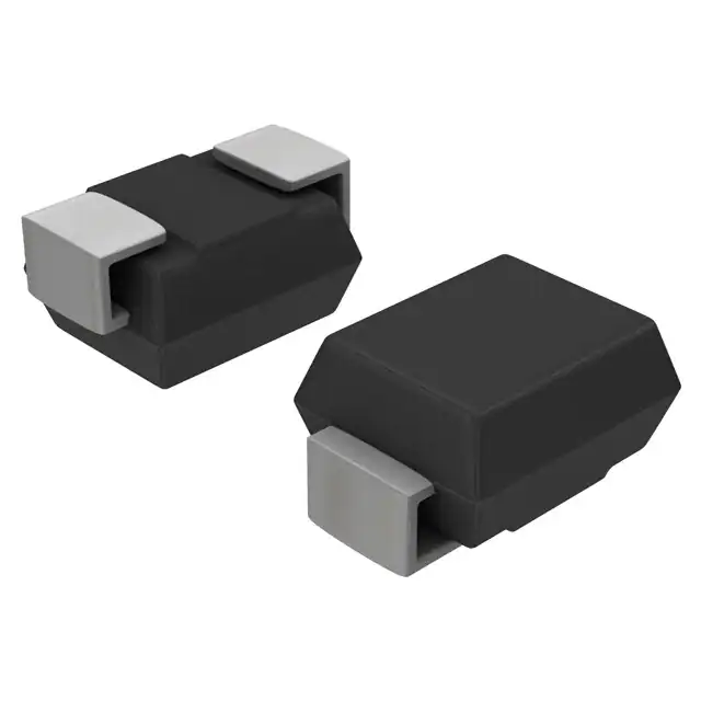
- Part No.:
- NP1800SBMCT3G
- Manufacturer:
- onsemi
- Category:
- Thyristors
- Package:
- DO-214AA, SMB
- Datasheet:
-
 NP1800SBMCT3G.pdf
- Description:
- THYRISTOR 170V 250A DO-214AA
- Quantity:
- Payment:

- Shipping:

Inventory:2,793
Please send an inquiry. Send us your inquiry, and we will respond immediately.
Product details
Overview
NP1800SBMCT3G from onsemi is a bidirectional ultra-low-capacitance thyristor surge protection device (TSPD) designed for telecom line protection in xDSL and T1/E1 interfaces. It features ±170 V repetitive peak off-state voltage (VDRM), ±220 V breakover voltage (V(BO)), 23 pF nominal off-state capacitance at 1 MHz, 4 V on-state voltage at 2.2 A peak, and 150 mA holding current - enabling transparent operation and fast crowbar clamping in high-speed data lines.
For engineers reviewing the NP1800SBMCT3G datasheet, pinout, applications, or equivalent options, this device is selected for precise overvoltage thresholding, minimal signal distortion in broadband transmission, compliance with GR-1089-CORE and ITU-T K.20/K.21, and robust 150 A non-repetitive surge current handling in SMB (DO-214AA) surface-mount packaging.
Technical Context
The NP1800SBMCT3G operates as a bidirectional crowbar-type protector: it remains high-impedance (open-circuit) under normal line conditions (IDRM ≤ 5 µA at VDRM), then switches to low-impedance (short-circuit) when transient voltage exceeds ±220 V (V(BO)), shunting surge energy to ground. Its ultra-low 23 pF off-state capacitance ensures <0.5% signal attenuation at 2.2 MHz, critical for ADSL2+ and E1 baseband integrity.
This TSPD uses silicon thyristor structure with controlled dv/dt immunity (≥100 V/µs) and thermal design supporting junction temperatures from −40°C to +150°C. The 90°C/W junction-to-ambient thermal resistance enables reliable operation in compact PCB layouts without forced airflow, validated per IEC 61000-4-5 Level 4 (4 kV) and TIA-968-A surge waveforms.
Key Specifications
| Parameter | Value and Actual Design Meaning |
|---|---|
| VDRM | ±170 V - Ensures stable open-circuit behavior up to telecom line peak voltages including 48 V DC battery + 150 V RMS ring (212 V peak), preventing false triggering. |
| V(BO) | ±220 V - Defines maximum clamping voltage seen by protected circuitry (e.g., SLIC or line interface IC), staying below typical 250 V failure thresholds. |
| Co (at 1 MHz) | 23 pF - Enables <−40 dB insertion loss at 2.2 MHz, preserving DSL upstream channel SNR and meeting ITU-T G.992.5 spectral mask requirements. |
| VT (at 2.2 A) | 4 V - Limits power dissipation to <9 W during 10×160 µs surges, avoiding thermal runaway in SMB package under 150 A peak pulse conditions. |
| IH | 150 mA - Guarantees automatic recovery to high-impedance state after surge decay, provided system load current remains <150 mA (e.g., idle-line monitoring circuits). |
| IPPS (10×160 µs) | 150 A - Supports GR-1089-CORE Category A (150 A) and TIA-968-A Level 3 (150 A) surge immunity without degradation across 1000 cycles. |
Pinout & Package
SMB (DO-214AA) surface-mount package per JEDEC standard, case 403C, with cathode/anode terminals on opposite ends of the molded body. Dimensions: 4.57 mm × 3.81 mm × 2.11 mm (L×W×H), 2.26 mm standoff height, 0.76–1.27 mm terminal width.
| Pin/Terminal | Circuit Role | Design Meaning |
|---|---|---|
| Anode (A) | Surge current entry point (bidirectional) | Connected to tip or ring line; conducts surge current toward cathode during either polarity overvoltage event. |
| Cathode (K) | Surge current exit point (bidirectional) | Typically tied to system ground or common return; completes low-impedance path during crowbar action. |
Key Features
| Feature | Design Value |
|---|---|
| Ultra-low off-state capacitance | 23 pF at 1 MHz - preserves signal integrity in >2 MHz broadband channels without requiring compensation networks. |
| Low leakage transparency | ≤5 µA IDRM at ±170 V - eliminates DC loading on line drivers and avoids false fault detection in monitoring circuits. |
| Precise bidirectional breakover | ±220 V V(BO) with ±5% tolerance - enables deterministic clamping margin between operating voltage (±170 V) and equipment failure threshold (±250 V). |
| High surge current capability | 150 A IPPS (10×160 µs) - meets GR-1089-CORE Category A and ITU-T K.21 Class B requirements without derating. |
| Pb-free RoHS-compliant construction | JEDEC-compliant SMB package with matte tin lead finish - supports lead-free reflow profiles (J-STD-020, peak 260°C) and eliminates post-solder cleaning. |
Applications
| xDSL Central Office Line Card | T1/E1 Data Interface Protection |
|---|---|
Use Scenario: Protecting ADSL2+ line drivers and receivers on central office DSLAM cards exposed to lightning-induced surges on copper loops up to 18,000 ft. IC Role / Device Role / Timing Role: Bidirectional crowbar protector placed differential across tip/ring before line transformer, clamping transients before they reach analog front-end ICs. Use Value: 23 pF capacitance prevents upstream channel degradation above 1.1 MHz; ±220 V V(BO) ensures clamping occurs before SLIC IC damage at ±250 V. |
Use Scenario: Safeguarding T1/E1 framer and transceiver ICs in telecom access equipment subjected to induced surges from adjacent power cables or switching noise. IC Role / Device Role / Timing Role: Primary overvoltage clamp on balanced 100 Ω twisted-pair interface, operating in parallel with gas discharge tubes for multi-stage protection. Use Value: 150 A surge rating handles TIA-968-A Level 3 (150 A) events; fast turn-on (<100 ns) limits voltage overshoot to <250 V during 10×160 µs transients. |
| Broadband Customer Premises Equipment | Industrial Ethernet over Copper |
Use Scenario: Integrated into residential DSL modems and gateways where space-constrained PCB layout demands minimal footprint and no external biasing. IC Role / Device Role / Timing Role: Standalone surge suppressor mounted directly at RJ-11 connector, providing first-line defense without series impedance or control logic. Use Value: SMB package fits 5.5 mm × 3.8 mm footprint; ±170 V VDRM accommodates 48 V DC phantom power plus AC ringing without leakage increase. |
Use Scenario: Protecting RS-485/RS-422 physical layer transceivers in factory automation systems connected via unshielded twisted pair in electrically noisy environments. IC Role / Device Role / Timing Role: Differential-mode protector across A/B bus lines, coordinated with common-mode chokes to meet IEC 61000-4-5 Level 3 (2 kV) requirements. Use Value: 90°C/W thermal resistance allows continuous operation at 85°C ambient; 150 mA IH ensures recovery after surge without latch-up in low-current bus idle states. |
Equivalent & Alternatives
The following parts are listed as comparable options for similar thyristor surge protection applications.
| Alternative Part | Technical Difference | Application Difference | Selection Advice |
|---|---|---|---|
| NP1800SCMC | Same electrical specs (VDRM, V(BO), Co, VT), but in SMC (DO-214AB) package - 7.11 mm × 6.22 mm footprint, 2.3× larger area than SMB. | Used where higher thermal mass is needed for repeated surge duty cycles; not suitable for dense xDSL line card layouts. | Select NP1800SCMC only if board space permits larger package and thermal budget exceeds 1.5 W sustained dissipation. |
| SM712-TR | TVS diode array (not thyristor); 12 V working voltage, 300 W peak power, 150 pF capacitance - lacks crowbar latching behavior and precise V(BO) threshold. | Applicable for low-voltage data lines (e.g., USB, RS-232); unsuitable for telecom line-level protection due to excessive capacitance and voltage mismatch. | NP1800SBMCT3G is required for telecom-grade differential line protection; SM712-TR serves only low-voltage, low-capacitance auxiliary ports. |
Compared with NP1800SCMC, the NP1800SBMCT3G offers identical protection performance in a 45% smaller footprint ideal for high-density line cards; versus SM712-TR, it delivers deterministic ±220 V clamping with 23 pF capacitance - essential for maintaining DSL spectral compliance where TVS leakage and capacitance would degrade upstream SNR.
Availability
NP1800SBMCT3G is available at Aetrix Electronics and suitable for xDSL infrastructure, T1/E1 telecom equipment, and industrial broadband data transmission systems requiring stable component supply, long-term lifecycle support, and RoHS-compliant manufacturing.
Supply support for NP1800SBMCT3G includes scheduled delivery planning, volume procurement assistance, BOM continuity management, traceable sourcing, and lifecycle availability coordination for OEM customers, industrial embedded developers, connected-device designers, and electronics production programs.
Manufacturer
onsemi (formerly ON Semiconductor) is a global semiconductor supplier specializing in energy-efficient power management, analog, sensor, and connectivity solutions for automotive, industrial, cloud, and communications markets.
The NPMC Series - including NP1800SBMCT3G - was engineered specifically for telecom line protection, delivering ultra-low capacitance and precise breakover voltage to meet GR-1089-CORE, ITU-T K.20/K.21, and IEC 61000-4-5 standards in space-constrained designs.
FAQ
What is the maximum continuous operating voltage for NP1800SBMCT3G?
The NP1800SBMCT3G has a repetitive peak off-state voltage (VDRM) of ±170 V, meaning it can continuously withstand up to ±170 V DC or peak AC voltage in the off-state without triggering. This rating ensures compatibility with telecom line voltages including 48 V DC battery feed plus 150 V RMS ringing (212 V peak), with 42 V safety margin below VDRM.
Does NP1800SBMCT3G require external bias or control circuitry?
No, the NP1800SBMCT3G is a passive, self-triggering thyristor device requiring no external bias, power, or control signals. It operates autonomously: remaining high-impedance until line voltage exceeds ±220 V (V(BO)), then latching into low-impedance conduction until current falls below 150 mA (IH). This simplifies protection design and eliminates single-point failure modes.
How does NP1800SBMCT3G compare to MOV-based protectors in telecom applications?
Unlike metal-oxide varistors (MOVs), the NP1800SBMCT3G provides precise ±220 V breakover voltage with <5% tolerance, ultra-low 23 pF capacitance, and no degradation after repeated surges. MOVs exhibit voltage drift, higher leakage, and capacitance >1 nF - causing unacceptable signal distortion in DSL and T1/E1 lines where NP1800SBMCT3G maintains spectral integrity.
Can NP1800SBMCT3G be used in AC mains protection?
No, the NP1800SBMCT3G is rated for telecom line protection only, with VDRM = ±170 V and thermal limits suited for short-duration surges (e.g., 10×160 µs). It is not designed for continuous AC mains exposure (120/230 V RMS), lacks UL 1449 certification for mains use, and would fail catastrophically under sustained overvoltage - use dedicated AC-rated TSPDs or GDTs instead.
What is the thermal resistance and maximum junction temperature of NP1800SBMCT3G?
The NP1800SBMCT3G has a junction-to-ambient thermal resistance (RθJA) of 90°C/W when mounted on a standard FR-4 PCB (3″×4.5″, 2 oz copper, 3×3 inch pad pattern). Its maximum junction temperature is +150°C, allowing reliable operation in industrial environments up to +85°C ambient when surge duty cycle remains below 0.1% - verified per JESD51-3 test conditions.
NP1800SBMCT3G Specifications
- Product attributes
- Attribute value
- Manufacturer:
- onsemi
- Package/Case:
- DO-214AA, SMB
- Series:
- -
- Packaging:
- Tape & Reel (TR)
- Product Status:
- Obsolete
- Voltage - Breakover:
- 220V
- Voltage - Off State:
- 170V
- Voltage - On State:
- 4 V
- Current - Peak Pulse (8/20µs):
- 250 A
- Current - Peak Pulse (10/1000µs):
- 80 A
- Current - Hold (Ih):
- 150 mA
- Number of Elements:
- 1
- Capacitance:
- 29pF
- Grade:
- -
- Qualification:
- -
- Mounting Type:
- Surface Mount
- Supplier Device Package:
- SMB
NP1800SBMCT3G FAQ
1.How can I place an order for NP1800SBMCT3G through Aetrix?
Please submit a Request for Quotation (RFQ) for NP1800SBMCT3G on Aetrix. Our sales agent will provide a competitive quotation and guide you through the order confirmation once you accept the terms.
2.Are the price and stock information for NP1800SBMCT3G reliable?
The price and inventory of NP1800SBMCT3G are updated periodically and may fluctuate due to market conditions. Stock and pricing data are typically refreshed every 24 hours. Quotation validity for NP1800SBMCT3G is usually 5 days.
3.What payment methods are accepted for NP1800SBMCT3G?
We accept Wire Transfer, PayPal, Credit Card, Western Union, MoneyGram, and Escrow for NP1800SBMCT3G transactions.
Note: Certain payment methods may incur a processing fee.
4.How is shipping managed for NP1800SBMCT3G?
NP1800SBMCT3G orders can be shipped via leading logistics carriers, including DHL, UPS, FedEx, TNT, or Registered Mail.
Once your NP1800SBMCT3G order is processed, you will receive an email with the shipment details and tracking number.
Note: Tracking information may take up to 24 hours to appear. Express delivery typically takes 3–5 business days.
5.How can I obtain technical support or documentation for NP1800SBMCT3G?
For technical support, including NP1800SBMCT3G datasheets, pinout diagrams, or application guidance, please contact our engineering support team. They can provide detailed documentation and assistance for your NP1800SBMCT3G requirements.
6.How does Aetrix verify that NP1800SBMCT3G is sourced from the original manufacturer or authorized distributors?
All NP1800SBMCT3G products on Aetrix are procured from qualified distributors and authorized channels. Our dedicated quality assurance team conducts strict verification, including traceability checks and, if necessary, third-party testing. This ensures that NP1800SBMCT3G meets industry standards.
7.What is the process for return or replacement of NP1800SBMCT3G?
All NP1800SBMCT3G units undergo pre-shipment inspection (PSI). If there is an issue with NP1800SBMCT3G, returns or replacements are accepted under the following conditions:
1.Quantity discrepancies, incorrect items, or visible external defects (such as breakage or corrosion), acknowledged by Aetrix.
2.The issue is reported within 90 days of delivery.
3.The NP1800SBMCT3G part is unused and in its original packaging.
Return procedure for NP1800SBMCT3G:
1.Submit a request within 90 days.
2.Obtain a Return Material Authorization (RMA) from Aetrix.
NP1800SBMCT3G Tags
-
TISP4015L1AJR-S
Bourns Inc.
-
TISP4015L1BJR-S
Bourns Inc.
-
SMP100LC-270
STMicroelectronics
-
TISP4240M3BJR-S
Bourns Inc.
-
SMP100LC-35
STMicroelectronics
-
SMP100LC-65
STMicroelectronics
-
SMP100LC-8
STMicroelectronics
-
TISP4P035L1NR-S
Bourns Inc.
-
TISP4350H3BJR-S
Bourns Inc.
-
TISP4011H1BJR-S
Bourns Inc.
-
SMP100LC-400
STMicroelectronics
-
P0300SALRP
Littelfuse Inc.
Tech Hub

Counterfeit components can hide behind convincing markings and passing basic function tests. This engineering reference covers source traceability, external inspection, X-ray, XRF, electrical testing, …

A practical engineering and sourcing framework covering lifecycle verification, lifetime-buy calculations, replacement qualification, supplier checks and counterfeit-risk controls.

TTL and CMOS logic families differ in thresholds, loading, output drive, power and timing. This engineering guide compares 74HC and 74HCT, calculates noise margins and checks 3.3 V/5 V compatibility.

A practical engineering guide to 3.3V and 5V logic compatibility, input thresholds, resistor dividers, translator ICs, MOSFET level shifting, I2C pull-ups, timing limits and power-sequencing risks.

The 74HC595 uses push-pull logic outputs, while the TPIC6B595 uses 50 V open-drain DMOS sinks for higher-power loads. This guide compares timing, current limits, 3.3 V interfacing, load wiring, thermal…

The 74HC595 converts serial data into eight stable parallel outputs. This guide covers pin functions, shift and storage timing, OE and MR behavior, drive-current limits, cascading, voltage compatibilit…

A technical comparison of level-sensitive latches and edge-triggered flip-flops, covering timing windows, setup and hold limits, master–slave operation, time borrowing, race-through, HDL inference and…

A D latch stores one bit while Enable controls when data can pass. This reference covers gate-level operation, truth tables, transparency, setup and hold timing, LE versus OE, common ICs and practical …

An SR latch stores one bit through cross-coupled feedback. This engineering reference covers NOR and NAND implementations, truth tables, forbidden-state recovery, gated operation, switch debouncing, fa…

Latch circuits retain one bit through feedback. This technical reference covers SR and D latches, truth tables, transparency, timing limits, latch-versus-flip-flop behavior, applications and common log…


