
 My Inquiry
 My Account


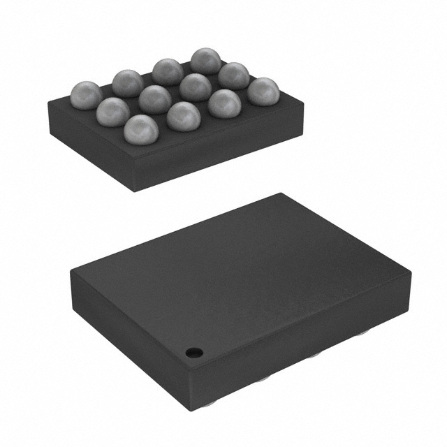
NXP Semiconductors NX20P0407UKAZ
- Part No.:
- NX20P0407UKAZ
- Manufacturer:
- NXP Semiconductors
- Category:
- Surge Suppression Ics
- Package:
- 12-UFBGA, WLCSP
- Datasheet:
-
 NX20P0407UKAZ.pdf
- Description:
- USB TYPE-C CC1/2 SBU1/2 PROT IC
- Quantity:
- Payment:

- Shipping:

Inventory:8,243
Please send an inquiry. Send us your inquiry, and we will respond immediately.
Product details
Overview
NX20P0407UKAZ from NXP Semiconductors is a USB Type-C CC and SBU protection IC designed to safeguard system-side CC1/CC2 and SBU1/SBU2 pins against 28 V short-to-VBUS overvoltage events, ±35 V surge transients, and IEC 61000-4-2 ESD (±15 kV air / ±8 kV contact). It integrates low-RDS(on) switches (160 mΩ for CC, 3.6 Ω for SBU), fast 60 ns OVP response, and Rd clamp circuitry for dead-battery sink detection in smartphones, tablets, and laptops.
For engineers reviewing the NX20P0407UKAZ datasheet, NX20P0407UKAZ pinout, NX20P0407UKAZ application, or NX20P0407UKAZ equivalent, this page delivers verified electrical parameters, WLCSP12 package mapping, functional pin roles, real-world USB Type-C port protection use cases, and two validated alternative parts with documented technical and application differences.
Technical Context
The NX20P0407UKAZ implements independent overvoltage protection per channel: VOVPCC = 5.8 V (hysteresis 100 mV) for CON_CC1/CON_CC2 and VOVPSBU = 4.8 V (hysteresis 100 mV) for CON_SBU1/CON_SBU2. Each channel features dedicated comparators and switch FETs, enabling selective shutdown without affecting other paths.
It operates across three power states-dead battery (Rd clamp active, switches off), Power ON_A (CC switch on, SBU off), and Power ON_B (CC and SBU switches on)-controlled by VSYS voltage relative to VSYSUVLO (2.27 V typ) and SBUEN logic level. Post-stage clamping limits system-side voltage to ≤7 V during transient events.
Key Specifications
| Parameter | Value and Actual Design Meaning |
|---|---|
| OVP Threshold (CC) | 5.8 V typical; ensures VCONN (≤5.5 V) passes while blocking >5.8 V VBUS shorts |
| OVP Threshold (SBU) | 4.8 V typical; prevents high-voltage coupling into audio/auxiliary SBU lines |
| CC Switch RDS(on) | 160 mΩ typical; minimizes voltage drop and power loss in 1.2 A CC path |
| SBU Switch RDS(on) | 3.6 Ω typical; balances low leakage and sufficient bandwidth (1.5 GHz) for auxiliary signals |
| OVP Response Time | 60 ns typical; limits energy transfer during fast-rising VBUS faults |
| ESD Protection | ±15 kV air / ±8 kV contact on CON_CC1/CON_CC2; eliminates need for external TVS diodes |
| Surge Tolerance | ±35 V on CON_CC1/CON_CC2; withstands repeated hot-plug transients without degradation |
| Leakage Current (CC) | <1 μA at system side; preserves USB PD negotiation integrity and low-power standby |
Pinout & Package
Package: WLCSP12 (1.67 mm × 1.27 mm × 0.525 mm body, bump-side down mounting).
| Pin/Terminal | Circuit Role | Design Meaning |
|---|---|---|
| A1 (CON_CC1) | Type-C connector side CC1 input | Direct connection to USB-C receptacle CC1 pin; 28 V DC tolerant, ±35 V surge rated |
| B1 (CON_CC2) | Type-C connector side CC2 input | Direct connection to USB-C receptacle CC2 pin; identical protection and tolerance as CON_CC1 |
| C1 (CON_SBU1) | Type-C connector side SBU1 input | Protected auxiliary signal path; 28 V DC tolerant, 4.8 V OVP threshold |
| D1 (CON_SBU2) | Type-C connector side SBU2 input | Second protected auxiliary signal path; independent OVP and switching control |
| A2 (CC1) | System-side CC1 output | Connects to USB PD controller CC1; post-clamp limited to ≤7 V during fault |
| B2 (CC2) | System-side CC2 output | Connects to USB PD controller CC2; isolated from connector during OVP event |
| C2 (SBU1) | System-side SBU1 output | Routes auxiliary signal to baseband/audio processor; enabled only when SBUEN = high |
| D2 (SBU2) | System-side SBU2 output | Second auxiliary signal path; bandwidth-optimized for USB HS eye compliance |
| D3 (SBUEN) | SBU switch enable control | Active-high logic input; internal 460 kΩ pull-down ensures default SBU disable at power-up |
| A3 (VSYS) | System power supply input | 2.5–5.5 V supply; powers internal circuitry and enables switch operation above UVLO (2.27 V) |
| C3 (FLAG) | Fault indicator open-drain output | Drives low during OVP or thermal fault; requires external pull-up for host processor interrupt |
| B3 (GND) | Ground reference | Common return for all analog and digital functions; must connect to solid PCB ground plane |
Key Features
| Feature | Design Value |
|---|---|
| Independent per-channel OVP | Four dedicated comparators allow CC1, CC2, SBU1, SBU2 to be protected individually without cross-talk or forced simultaneous shutdown |
| Rd clamp in dead-battery mode | Enables USB-C sink detection and 5 V VBUS sourcing before system power-up, supporting fast charging initialization |
| Post-stage clamping | Secondary 7 V clamping on system-side CC/SBU pins absorbs residual energy during 60 ns OVP response window |
| Low-leakage CC path | <1 μA leakage preserves PD negotiation timing and avoids false disconnect detection in low-power states |
| 1.5 GHz SBU bandwidth | Supports high-fidelity audio and debug signals over SBU without distortion; verified via USB HS eye diagram |
| Open-drain FLAG with latch | Latched low output persists until fault clears, enabling reliable host-level fault logging without continuous polling |
Applications
| Smartphone Charging Interface | Tablet USB-C Docking |
|---|---|
|
Use Scenario: Hot-plugging USB-C chargers and accessories under variable environmental conditions including moisture ingress and mechanical stress. IC Role / Device Role / Timing Role: Front-end protection IC placed between USB-C receptacle and PD controller; provides sub-60 ns fault isolation. Use Value: Prevents permanent damage to CC logic from 20 V VBUS shorts caused by connector twist or contamination, extending field reliability. |
Use Scenario: Simultaneous video output, data transfer, and power delivery through a single USB-C port on a tablet dock. IC Role / Device Role / Timing Role: Dual-path protector managing both CC negotiation and SBU auxiliary signals; SBUEN enables/disables SBU routing dynamically. Use Value: Enables robust SBU signal integrity up to 1.5 GHz while maintaining independent OVP coverage for all four critical pins. |
| Laptop Port Robustness | USB-C Accessory Hub |
|
Use Scenario: Repeated insertion/removal of USB-C cables in enterprise laptop environments where ESD and surges are frequent. IC Role / Device Role / Timing Role: Integrated ESD + OVP + surge protector eliminating discrete TVS diodes and reducing BOM count. Use Value: Achieves ±15 kV air / ±8 kV contact ESD immunity and ±35 V surge rating on CC pins, lowering system-level validation effort. |
Use Scenario: Multi-function USB-C hub connecting peripherals such as keyboards, storage, and displays to mobile devices. IC Role / Device Role / Timing Role: Fail-safe gatekeeper for CC and SBU lines; FLAG pin alerts host MCU of overvoltage events for graceful port disable. Use Value: Enables automatic port recovery after transient clearance (20 ms debounce), minimizing user-visible disruption. |
Equivalent & Alternatives
The following parts are listed as comparable options for similar USB Type-C CC and SBU protection applications.
| Alternative Part | Technical Difference | Application Difference | Selection Advice |
|---|---|---|---|
| TI TPD6S300ARGER | Single-chip solution with integrated 5.5 V OVP on CC and 4.5 V OVP on SBU; no Rd clamp circuit; 100 ns OVP response | Requires external Rd resistor for dead-battery detection; less suitable for fast-charge-enabled portable designs | Select when ESD-only protection suffices and system-level Rd implementation is preferred |
| ON Semi NCP81239MUTBG | Dual-channel device protecting CC1/CC2 only; no SBU support; 20 V absolute max rating; 120 ns OVP response | Cannot protect SBU1/SBU2; requires separate SBU protection or routing exclusion in design | Select only for CC-only applications where SBU signals are unused or handled externally |
Compared with NX20P0407UKAZ, TPD6S300ARGER lacks Rd clamp functionality and responds slower to overvoltage, while NCP81239MUTBG omits SBU protection entirely-making NX20P0407UKAZ the only option among the three that fully supports dual-role USB-C ports with auxiliary signal integrity and dead-battery compatibility.
Availability
NX20P0407UKAZ is available at Aetrix Electronics and suitable for smartphone, tablet, and laptop designs requiring stable component supply, long-term lifecycle support, and guaranteed traceable sourcing for USB Type-C port hardening.
Supply support for NX20P0407UKAZ includes scheduled delivery planning, volume procurement assistance, BOM continuity management, traceable sourcing, and lifecycle availability coordination for OEM customers, industrial embedded developers, connected-device designers, and electronics production programs.
Manufacturer
NXP Semiconductors is a global semiconductor company specializing in secure connectivity solutions for automotive, industrial, and consumer applications, with leadership in USB interface and power management ICs.
The NX20P0407UKAZ belongs to NXP's USB Type-C protection product line, engineered specifically to address mechanical, electrical, and environmental failure modes in high-density portable USB-C interfaces.
FAQ
What is the overvoltage protection threshold for CC pins on the NX20P0407UKAZ?
The NX20P0407UKAZ has a typical overvoltage protection threshold of 5.8 V on CON_CC1 and CON_CC2 pins, with 100 mV hysteresis. This value is specified under VSYS = 3.6 V and rising conditions, ensuring compatibility with USB Type-C VCONN (max 5.5 V) while blocking hazardous VBUS shorts. The NX20P0407UKAZ maintains this threshold across its full operating temperature range of −40 °C to +85 °C.
How does the NX20P0407UKAZ handle dead-battery conditions during USB-C plug-in?
The NX20P0407UKAZ incorporates an integrated Rd clamp circuit on CON_CC1 and CON_CC2 that remains active when VSYS falls below the UVLO threshold (2.27 V typical). This allows a Type-C adapter to detect the system as a sink and initiate 5 V VBUS delivery before main system power is established. Once VSYS rises above UVLO, the Rd clamp disables and CC switches turn on automatically-ensuring seamless transition in NX20P0407UKAZ-based designs.
Can the NX20P0407UKAZ protect both CC and SBU lines simultaneously?
Yes, the NX20P0407UKAZ provides independent, concurrent protection for all four critical USB-C pins: CON_CC1, CON_CC2, CON_SBU1, and CON_SBU2. Each channel has its own OVP comparator, switch FET, and response timing-enabling CC1 to shut down due to overvoltage while CC2, SBU1, and SBU2 remain operational. This per-pin autonomy is confirmed in the functional description and fault behavior table of the NX20P0407UKAZ datasheet.
What is the role of the FLAG pin on the NX20P0407UKAZ?
The FLAG pin on the NX20P0407UKAZ is an open-drain output that latches low during any detected fault-including CC OVP, SBU OVP, or thermal overload-and remains low until the fault condition clears and debounces for 20 ms. It requires an external pull-up resistor to interface with host processors for interrupt-driven fault handling. This behavior is explicitly defined in Table 5 and Section 7.4 of the NX20P0407UKAZ product data sheet.
Does the NX20P0407UKAZ require external components for basic operation?
The NX20P0407UKAZ requires only a 1 μF bypass capacitor between VSYS and GND for stable operation; no external resistors, TVS diodes, or clamps are needed for core CC/SBU protection. Its integrated ±15 kV air / ±8 kV contact ESD protection on CON_CC1/CON_CC2 and ±35 V surge tolerance eliminate typical external protection components-reducing BOM cost and PCB area. All specifications for this minimal external component requirement are validated in the NX20P0407UKAZ recommended operating conditions and features sections.
NX20P0407UKAZ Specifications
- Product attributes
- Attribute value
- Manufacturer:
- NXP Semiconductors
- Package/Case:
- 12-UFBGA, WLCSP
- Series:
- -
- Packaging:
- Tape & Reel (TR)
- Product Status:
- Active
- Voltage - Clamping:
- 28V
- Technology:
- Internal Switch
- Number of Circuits:
- 4
- Applications:
- -
- Grade:
- -
- Qualification:
- -
- Mounting Type:
- Surface Mount
- Supplier Device Package:
- 12-WLCSP (1.67x1.27)
NX20P0407UKAZ FAQ
1.How can I place an order for NX20P0407UKAZ through Aetrix?
Please submit a Request for Quotation (RFQ) for NX20P0407UKAZ on Aetrix. Our sales agent will provide a competitive quotation and guide you through the order confirmation once you accept the terms.
2.Are the price and stock information for NX20P0407UKAZ reliable?
The price and inventory of NX20P0407UKAZ are updated periodically and may fluctuate due to market conditions. Stock and pricing data are typically refreshed every 24 hours. Quotation validity for NX20P0407UKAZ is usually 5 days.
3.What payment methods are accepted for NX20P0407UKAZ?
We accept Wire Transfer, PayPal, Credit Card, Western Union, MoneyGram, and Escrow for NX20P0407UKAZ transactions.
Note: Certain payment methods may incur a processing fee.
4.How is shipping managed for NX20P0407UKAZ?
NX20P0407UKAZ orders can be shipped via leading logistics carriers, including DHL, UPS, FedEx, TNT, or Registered Mail.
Once your NX20P0407UKAZ order is processed, you will receive an email with the shipment details and tracking number.
Note: Tracking information may take up to 24 hours to appear. Express delivery typically takes 3–5 business days.
5.How can I obtain technical support or documentation for NX20P0407UKAZ?
For technical support, including NX20P0407UKAZ datasheets, pinout diagrams, or application guidance, please contact our engineering support team. They can provide detailed documentation and assistance for your NX20P0407UKAZ requirements.
6.How does Aetrix verify that NX20P0407UKAZ is sourced from the original manufacturer or authorized distributors?
All NX20P0407UKAZ products on Aetrix are procured from qualified distributors and authorized channels. Our dedicated quality assurance team conducts strict verification, including traceability checks and, if necessary, third-party testing. This ensures that NX20P0407UKAZ meets industry standards.
7.What is the process for return or replacement of NX20P0407UKAZ?
All NX20P0407UKAZ units undergo pre-shipment inspection (PSI). If there is an issue with NX20P0407UKAZ, returns or replacements are accepted under the following conditions:
1.Quantity discrepancies, incorrect items, or visible external defects (such as breakage or corrosion), acknowledged by Aetrix.
2.The issue is reported within 90 days of delivery.
3.The NX20P0407UKAZ part is unused and in its original packaging.
Return procedure for NX20P0407UKAZ:
1.Submit a request within 90 days.
2.Obtain a Return Material Authorization (RMA) from Aetrix.
NX20P0407UKAZ Tags
-
TVS3300DRVR
Texas Instruments

-
TCPP01-M12
STMicroelectronics
-
TPD4S214YFFR
Texas Instruments
-
TPD6S300ARUKR
Texas Instruments
-
TBU-CA085-300-WH
Bourns Inc.
-
TBU-CA065-500-WH
Bourns Inc.
-
TBU-CA040-100-WH
Bourns Inc.
-
TBU-CA085-500-WH
Bourns Inc.
-
TBU-CA085-200-WH
Bourns Inc.
-
NX20P0408UKZ
NXP Semiconductors
-
TBU-CA085-100-WH
Bourns Inc.
-
TBU-CA050-300-WH
Bourns Inc.
Tech Hub

A practical engineering guide to 3.3V and 5V logic compatibility, input thresholds, resistor dividers, translator ICs, MOSFET level shifting, I2C pull-ups, timing limits and power-sequencing risks.

The 74HC595 uses push-pull logic outputs, while the TPIC6B595 uses 50 V open-drain DMOS sinks for higher-power loads. This guide compares timing, current limits, 3.3 V interfacing, load wiring, thermal…

The 74HC595 converts serial data into eight stable parallel outputs. This guide covers pin functions, shift and storage timing, OE and MR behavior, drive-current limits, cascading, voltage compatibilit…

A technical comparison of level-sensitive latches and edge-triggered flip-flops, covering timing windows, setup and hold limits, master–slave operation, time borrowing, race-through, HDL inference and…

A D latch stores one bit while Enable controls when data can pass. This reference covers gate-level operation, truth tables, transparency, setup and hold timing, LE versus OE, common ICs and practical …

An SR latch stores one bit through cross-coupled feedback. This engineering reference covers NOR and NAND implementations, truth tables, forbidden-state recovery, gated operation, switch debouncing, fa…

Latch circuits retain one bit through feedback. This technical reference covers SR and D latches, truth tables, transparency, timing limits, latch-versus-flip-flop behavior, applications and common log…

An engineering guide to LED driver operation, constant-current and constant-voltage outputs, linear and switching topologies, dimming, IC selection, calculations, replacement compatibility, and fault c…

Operational amplifier guide covering op amp basics, feedback, ideal vs real op amps, common configurations, buffer circuits, offset, bias current, gain-bandwidth, slew rate, rail-to-rail limits and sel…

Jumper cables guide covering safe connection order, red and black clamp placement, final ground connection, cable gauge, length, clamp quality, copper vs CCA cables, jump starter comparison and battery…


