
 My Inquiry
 My Account


STMicroelectronics OCVPB21-13F6
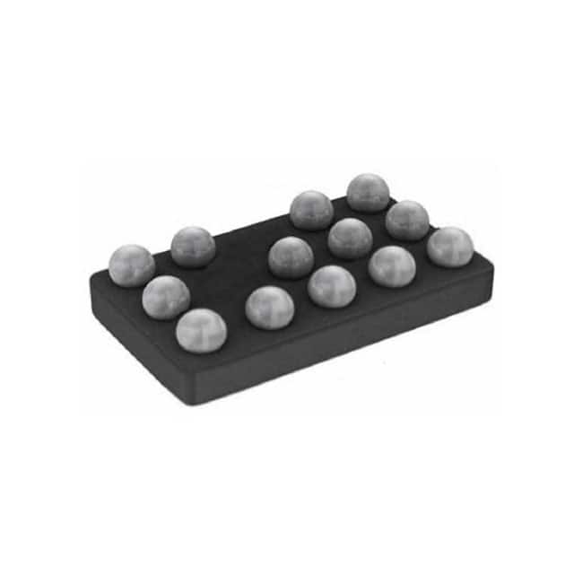
- Part No.:
- OCVPB21-13F6
- Manufacturer:
- STMicroelectronics
- Category:
- Surge Suppression Ics
- Package:
- 13-UFBGA, WLCSP
- Datasheet:
-
 OCVPB21-13F6.pdf
- Description:
- ESD, OVERVOLTAGE AND OVERCURRENT
- Quantity:
- Payment:

- Shipping:

Inventory:9,879
Please send an inquiry. Send us your inquiry, and we will respond immediately.
Product details
Overview
OCVPB21-13F6 from STMicroelectronics is a highly integrated USB interface protection IC with 13 V input rectification bridge, ±15 kV IEC 61000-4-2 ESD protection on bridge inputs, adjustable 100–500 mA overcurrent protection, 5 V USB 2.0 data-line multiplexing (RON = 6 Ω typ), and open-drain FLAG output for fault reporting-designed for battery charging circuits in wearables and IoT devices where cable polarity inversion must be handled autonomously.
For engineers reviewing the OCVPB21-13F6 datasheet, OCVPB21-13F6 pinout, OCVPB21-13F6 application, or OCVPB21-13F6 equivalent, this device delivers verified USB cable orientation detection, bidirectional 13 V OVP (-0.3 V to +13.2 V), thermal shutdown at 148 °C, and WLCSP-13 package compatibility with 400 µm pitch-critical for space-constrained portable power management designs.
Technical Context
The OCVPB21-13F6 integrates a high-voltage rectification bridge that detects USB cable polarity via IN_A/IN_B inputs and reroutes USB_DP/USB_DM signals accordingly-enabling correct D+/D− mapping regardless of plug orientation. Its internal charge-pump-driven high-side/low-side MOSFET gate drivers support low-drop conduction (RON = 199 mΩ high-side, 119 mΩ low-side) while maintaining robust ESD immunity across all pins.
Overcurrent protection is externally set via RLIM (51–270 Ω), yielding precise ILIM from 108 mA to 586 mA; fast short-circuit response folds back current to ~75 mA, and thermal shutdown (Tsd = 148 °C, hysteresis = 28 °C) disables the switch until junction temperature drops by 30 °C-ensuring safe operation under sustained overload.
Key Specifications
| Parameter | Value and Actual Design Meaning |
|---|---|
| ESD Protection | ±15 kV contact on bridge inputs (IN_A/IN_B), ±12 kV on USB data lines per IEC 61000-4-2 Level 4-enables direct USB connector interfacing without external TVS diodes |
| OVP Range | -0.3 V to +13.2 V DC input tolerance with 5.5 V OVLO activation-protects downstream PMICs during voltage transients and ringing up to 20 V |
| OCP Adjustment | 100–500 mA via external RLIM resistor (51–270 Ω)-supports flexible current limiting for diverse wearable battery chemistries and charge profiles |
| Data Path RON | 6 Ω typical (9.2 Ω max) with 1.6 Ω flatness-preserves USB 2.0 signal integrity (480 Mbps eye diagram compliant) and minimizes insertion loss |
| Operating Temp | -30 °C to +65 °C ambient range-validated for continuous use in thermally constrained wearable enclosures and ambient-exposed IoT housings |
| Package | WLCSP-13, 1.32 mm × 2.10 mm, 400 µm pitch, 605 µm thickness-enables <2.8 mm² PCB footprint for ultra-thin form factors |
Pinout & Package
OCVPB21-13F6 uses a 13-bump WLCSP package with 400 µm pitch, optimized for flip-chip mounting on high-density wearable PCBs. Bump layout follows standard A–E row / 1–3 column grid with non-solder-mask-defined microvias recommended.
| Pin/Terminal | Circuit Role | Design Meaning |
|---|---|---|
| A1 | USB_DP (OUT_USB_D+) | Output USB D+ data line after polarity correction-drives downstream USB transceiver with ≤9 pF capacitance |
| A2 | USB_IND | Input USB dataline (D− or D+) from connector-routed through internal MUX based on bridge polarity detection |
| A3 | GND_DATA | Dataline ground reference-separate from bridge/ESD grounds to minimize noise coupling into high-speed data paths |
| B1 | USB_DM (OUT_USB_D−) | Output USB D− data line after polarity correction-maintains 90 Ω differential impedance with A1 |
| B2 | OUT_5V | Regulated 5 V output to battery charger IC-delivers up to 600 mA with UVLO/OVLO protection and controlled inrush |
| B3 | USB_INC | Input USB dataline (D− or D+) from connector-paired with A2 to determine cable orientation via bridge logic |
| C2 | RECTIF | Bridge rectification output-connects to internal LDO and OVP circuitry; enables polarity-agnostic power path |
| D1 | IN_A | Bridge input (VCC or GND from USB connector)-forms one leg of 13 V rectifier; body diode conducts during startup |
| D3 | IN_B | Bridge input (GND or VCC from USB connector)-completes polarity detection; MOSFETs conduct in steady state |
| E1 | RLIM | OCP threshold setting node-accepts external resistor (51–270 Ω) to program current limit from 100–500 mA |
| E2 | GND_BRIDGE | Bridge ground reference-electrically isolated from GND_ESD and GND_DATA to prevent ESD current injection into analog blocks |
| E3 | FLAG | Open-drain fault indicator-asserted low during OCP, OVP, OTP, or incomplete startup; requires external pull-up |
| C3 | GND_ESD | ESD protection ground-provides dedicated low-inductance return path for ±15 kV ESD currents on power/data lines |
Key Features
| Feature | Design Value |
|---|---|
| USB Cable Polarity Detection & Correction | Integrated 13 V rectification bridge reroutes USB_DP/USB_DM automatically-eliminates need for mechanical keyed connectors or manual orientation checks |
| Programmable Overcurrent Protection | External RLIM resistor sets precise 100–500 mA trip point with ±15% accuracy-enables single BOM part across multiple battery capacity variants |
| Multi-Threshold Fault Reporting | Single FLAG pin signals OCP, OVP, OTP, and startup failure-reduces GPIO count and simplifies host MCU fault-handling firmware |
| USB 2.0 Signal Integrity Preservation | 9 pF ON capacitance, 420 MHz -3 dB bandwidth, and 9.2 Ω RON-meets USB-IF eye diagram requirements without external equalization |
| Thermal Robustness in Thin Form Factors | 148 °C thermal shutdown with 28 °C hysteresis and 605 µm package thickness-prevents thermal runaway in sealed wearable enclosures |
Applications
| Smart Band Charging Interface | Fitness Tracker Power Management |
|---|---|
|
Use Scenario: USB-C cable used interchangeably in either orientation to charge a wrist-worn smart band with Li-ion battery. IC Role / Device Role / Timing Role: Front-end protection and polarity correction IC placed between USB connector and buck-boost charger IC. Use Value: Eliminates mechanical orientation dependency and prevents reverse-voltage damage to 5 V PMIC; supports 480 Mbps USB data passthrough for firmware updates. |
Use Scenario: Compact fitness tracker subjected to repeated plugging/unplugging in uncontrolled environments (e.g., gym, travel). IC Role / Device Role / Timing Role: Integrated ESD/OVP/OCP guard protecting sensitive battery fuel gauge and charging controller from transient surges. Use Value: Withstands ±15 kV ESD strikes without latch-up; maintains <100 ns OCP response to prevent PMIC overcurrent damage during hot-plug events. |
| Wireless Earbud Case Charging | Medical Wearable Sensor Hub |
|
Use Scenario: Small-form-factor earbud charging case with minimal PCB area, requiring USB power delivery and data communication. IC Role / Device Role / Timing Role: USB interface protector enabling simultaneous 5 V power delivery and USB 2.0 data transfer to embedded MCU. Use Value: 2.77 mm² WLCSP footprint saves >30% board area vs. discrete protection solutions; 6 Ω RON ensures <50 mV data-line voltage drop at 8 mA. |
Use Scenario: FDA-classified medical wearable monitoring vital signs, requiring reliable USB charging under clinical environmental stress. IC Role / Device Role / Timing Role: Safety-critical front-end protector ensuring no overvoltage (>5.5 V) or reverse polarity reaches patient-connected battery management system. Use Value: Dual OVP/UVLO thresholds (5.5 V / 4.25 V) guarantee charger disable before battery overcharge; FLAG signal triggers safety shutdown in host MCU. |
Equivalent & Alternatives
The following parts are listed as comparable options for similar USB interface protection applications.
| Alternative Part | Technical Difference | Application Difference | Selection Advice |
|---|---|---|---|
| TPD2S017DRBR | Lower ESD rating (±8 kV HBM, ±12 kV IEC); no rectification bridge; fixed 1.2 A OCP; no FLAG output | Requires external polarity detection circuitry; limited to fixed-current applications; lacks fault signaling | Choose only if ESD requirements are ≤±12 kV and cable inversion is mechanically prevented |
| MAX14541EATA+ | No integrated rectifier; ±15 kV IEC ESD; 100–1200 mA OCP; FLAG output; 1.8 V to 5.5 V operation | Cannot handle USB cable reversal; wider input voltage range but no 13 V OVP clamping | Select when operating from non-USB sources (e.g., 3.3 V supply) and polarity is guaranteed |
Compared with TPD2S017DRBR and MAX14541EATA+, OCVPB21-13F6 uniquely combines 13 V rectification, ±15 kV ESD, programmable OCP, and unified FLAG reporting in a sub-3 mm² package-making it the only solution qualified for unattended USB cable orientation in certified wearable designs.
Availability
OCVPB21-13F6 is available at Aetrix Electronics and suitable for wearable device charging interfaces, IoT sensor node power management, and compact medical electronics requiring stable component supply with full lifecycle traceability.
Supply support for OCVPB21-13F6 includes scheduled delivery planning, volume procurement assistance, BOM continuity management, traceable sourcing, and lifecycle availability coordination for OEM customers, industrial embedded developers, connected-device designers, and electronics production programs.
Manufacturer
STMicroelectronics is a global semiconductor leader headquartered in Geneva, Switzerland, specializing in intelligent power, sensing, and control technologies for automotive, industrial, and consumer markets.
OCVPB21-13F6 belongs to ST's USB interface protection product line, engineered specifically to address polarity-agnostic charging, high-voltage transient resilience, and ultra-compact integration needs in next-generation wearables and edge IoT endpoints.
FAQ
What is the purpose of the RECTIF pin?
The RECTIF pin outputs the rectified voltage from the internal 13 V bridge, serving as the primary power source for the internal LDO regulator and OVP circuitry. It ensures stable biasing regardless of USB cable orientation and provides the reference for polarity detection logic-enabling automatic rerouting of USB data lines without external control signals.
How does the RLIM resistor affect overcurrent protection accuracy?
RLIM sets the OCP threshold using the formula ILIM = (318 − RLIM)/0.447 (mA). A 1% tolerance resistor yields ±15% current limit accuracy due to process variation in the internal current-sense amplifier. For tight regulation, ST recommends placing RLIM within 2 mm of the E1 pin with Z < 500 mΩ trace impedance to minimize noise-induced trip errors.
Can OCVPB21-13F6 support USB 2.0 high-speed data without signal degradation?
Yes-its 9 pF ON capacitance, 420 MHz -3 dB bandwidth, and 9.2 Ω RON meet USB-IF high-speed (480 Mbps) eye diagram specifications. The internal MUX preserves differential impedance matching, and layout guidelines specify 90 Ω differential routing for USB_INC/USB_IND/USB_DP/USB_DM traces to maintain signal integrity.
What happens during thermal shutdown and how is recovery managed?
When junction temperature reaches 148 °C, the power switch opens and FLAG goes low. Recovery begins only after temperature drops by 28 °C (hysteresis), re-enabling the output. This prevents thermal cycling; the 605 µm WLCSP package's thermal resistance (θJA ≈ 180 °C/W) ensures safe cooldown within seconds under typical wearable PCB copper pour conditions.
OCVPB21-13F6 Specifications
- Product attributes
- Attribute value
- Manufacturer:
- STMicroelectronics
- Package/Case:
- 13-UFBGA, WLCSP
- Series:
- -
- Packaging:
- Tape & Reel (TR)
- Product Status:
- Active
- Voltage - Clamping:
- 13V
- Technology:
- Internal Switch
- Number of Circuits:
- 1
- Applications:
- General Purpose
- Grade:
- -
- Qualification:
- -
- Mounting Type:
- Surface Mount
- Supplier Device Package:
- 13-WLCSP (2.1x1.32)
OCVPB21-13F6 FAQ
1.How can I place an order for OCVPB21-13F6 through Aetrix?
Please submit a Request for Quotation (RFQ) for OCVPB21-13F6 on Aetrix. Our sales agent will provide a competitive quotation and guide you through the order confirmation once you accept the terms.
2.Are the price and stock information for OCVPB21-13F6 reliable?
The price and inventory of OCVPB21-13F6 are updated periodically and may fluctuate due to market conditions. Stock and pricing data are typically refreshed every 24 hours. Quotation validity for OCVPB21-13F6 is usually 5 days.
3.What payment methods are accepted for OCVPB21-13F6?
We accept Wire Transfer, PayPal, Credit Card, Western Union, MoneyGram, and Escrow for OCVPB21-13F6 transactions.
Note: Certain payment methods may incur a processing fee.
4.How is shipping managed for OCVPB21-13F6?
OCVPB21-13F6 orders can be shipped via leading logistics carriers, including DHL, UPS, FedEx, TNT, or Registered Mail.
Once your OCVPB21-13F6 order is processed, you will receive an email with the shipment details and tracking number.
Note: Tracking information may take up to 24 hours to appear. Express delivery typically takes 3–5 business days.
5.How can I obtain technical support or documentation for OCVPB21-13F6?
For technical support, including OCVPB21-13F6 datasheets, pinout diagrams, or application guidance, please contact our engineering support team. They can provide detailed documentation and assistance for your OCVPB21-13F6 requirements.
6.How does Aetrix verify that OCVPB21-13F6 is sourced from the original manufacturer or authorized distributors?
All OCVPB21-13F6 products on Aetrix are procured from qualified distributors and authorized channels. Our dedicated quality assurance team conducts strict verification, including traceability checks and, if necessary, third-party testing. This ensures that OCVPB21-13F6 meets industry standards.
7.What is the process for return or replacement of OCVPB21-13F6?
All OCVPB21-13F6 units undergo pre-shipment inspection (PSI). If there is an issue with OCVPB21-13F6, returns or replacements are accepted under the following conditions:
1.Quantity discrepancies, incorrect items, or visible external defects (such as breakage or corrosion), acknowledged by Aetrix.
2.The issue is reported within 90 days of delivery.
3.The OCVPB21-13F6 part is unused and in its original packaging.
Return procedure for OCVPB21-13F6:
1.Submit a request within 90 days.
2.Obtain a Return Material Authorization (RMA) from Aetrix.
OCVPB21-13F6 Tags
-
TVS3300DRVR
Texas Instruments

-
TCPP01-M12
STMicroelectronics
-
TPD4S214YFFR
Texas Instruments
-
TPD6S300ARUKR
Texas Instruments
-
TBU-CA085-300-WH
Bourns Inc.
-
TBU-CA065-500-WH
Bourns Inc.
-
TBU-CA040-100-WH
Bourns Inc.
-
TBU-CA085-500-WH
Bourns Inc.
-
TBU-CA085-200-WH
Bourns Inc.
-
NX20P0408UKZ
NXP Semiconductors
-
TBU-CA085-100-WH
Bourns Inc.
-
TBU-CA050-300-WH
Bourns Inc.
Tech Hub

A practical engineering guide to 3.3V and 5V logic compatibility, input thresholds, resistor dividers, translator ICs, MOSFET level shifting, I2C pull-ups, timing limits and power-sequencing risks.

The 74HC595 uses push-pull logic outputs, while the TPIC6B595 uses 50 V open-drain DMOS sinks for higher-power loads. This guide compares timing, current limits, 3.3 V interfacing, load wiring, thermal…

The 74HC595 converts serial data into eight stable parallel outputs. This guide covers pin functions, shift and storage timing, OE and MR behavior, drive-current limits, cascading, voltage compatibilit…

A technical comparison of level-sensitive latches and edge-triggered flip-flops, covering timing windows, setup and hold limits, master–slave operation, time borrowing, race-through, HDL inference and…

A D latch stores one bit while Enable controls when data can pass. This reference covers gate-level operation, truth tables, transparency, setup and hold timing, LE versus OE, common ICs and practical …

An SR latch stores one bit through cross-coupled feedback. This engineering reference covers NOR and NAND implementations, truth tables, forbidden-state recovery, gated operation, switch debouncing, fa…

Latch circuits retain one bit through feedback. This technical reference covers SR and D latches, truth tables, transparency, timing limits, latch-versus-flip-flop behavior, applications and common log…

An engineering guide to LED driver operation, constant-current and constant-voltage outputs, linear and switching topologies, dimming, IC selection, calculations, replacement compatibility, and fault c…

Operational amplifier guide covering op amp basics, feedback, ideal vs real op amps, common configurations, buffer circuits, offset, bias current, gain-bandwidth, slew rate, rail-to-rail limits and sel…

Jumper cables guide covering safe connection order, red and black clamp placement, final ground connection, cable gauge, length, clamp quality, copper vs CCA cables, jump starter comparison and battery…


