
 My Inquiry
 My Account


Renesas P9025AC-RNBGI8
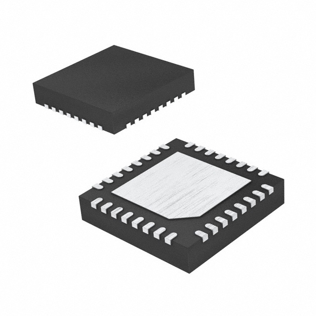
- Part No.:
- P9025AC-RNBGI8
- Manufacturer:
- Renesas
- Category:
- Power Management - Specialized
- Package:
- 32-WFQFN Exposed Pad
- Datasheet:
-
 P9025AC-RNBGI8.pdf
- Description:
- IC WIRELESS PWR RECEIVER 32VFQFN
- Quantity:
- Payment:

- Shipping:

Inventory:4,895
Please send an inquiry. Send us your inquiry, and we will respond immediately.
Product details
Overview
P9025AC-RNBGI8 from Integrated Device Technology is a WPC-1.1.2-compliant 5W Qi wireless power receiver IC with integrated full-bridge synchronous rectifier and 5.3V/1A LDO output. It operates across 0°C to +85°C, delivers regulated output via closed-loop power transfer control, and implements programmable foreign object detection (FOD) using dual external resistors (FOD1/FOD2). It serves as the core receiver in battery-powered electronics requiring contactless charging.
For engineers reviewing the P9025AC-RNBGI8 datasheet, P9025AC-RNBGI8 pinout, P9025AC-RNBGI8 application, or P9025AC-RNBGI8 equivalent, key selection criteria include its 5.3V LDO output voltage tolerance (±4.7%), I²C-accessible rectifier voltage and resonance frequency, programmable 1.15–1.95A current limit via RLIM, and advanced FOD compensation using OTP-stored curves and volatile I²C override.
Technical Context
The P9025AC-RNBGI8 integrates a synchronous full-bridge rectifier that transitions from body-diode conduction to half/full-synchronous mode once VRECT exceeds 7V, dynamically adjusting rectifier voltage targets (5.45V–7V) based on load current to optimize LDO efficiency. Its internal multi-channel ADC digitizes VRECT and output current for real-time closed-loop control of transmitter frequency and power level.
Communication follows WPC v1.1.2 differential bi-phase encoding at 2 kHz, enabling Rx-to-Tx packets including Signal Strength, Identification, Configuration, Control Error, Rectified Power, and End-of-Power. FOD relies on precise received-power measurement and system-loss compensation via 10 OTP-programmed curves selected by FOD1 resistor value, plus ±300 mW offset tuning via FOD2 resistor.
Key Specifications
| Parameter | Value and Actual Design Meaning |
|---|---|
| VOUT | 5.3V nominal, ±4.7% tolerance over 0–1000 mA load ensures stable supply for USB-5V peripherals despite LDO headroom loss. |
| ILIM | Programmable 1.15–1.95A via RLIM = 30 kΩ; enables safe 1A operation while supporting transient peaks without external current sensing. |
| VRECT Range | 5.45–7V target window, stepped by load current region; minimizes LDO dropout loss and improves thermal margin under varying loads. |
| FOD Resolution | 10 OTP-stored compensation curves + volatile I²C override + ±300 mW FOD2 offset; allows precise calibration against system-specific parasitic losses. |
| I²C Interface | 400 kHz max clock, open-drain SCL/SDA with 2.2 kΩ pull-ups to OUT; provides real-time access to rectifier voltage, output current, and resonance frequency for host monitoring. |
| Thermal Shutdown | 150°C trip / 130°C hysteresis; protects die during sustained overload or poor PCB thermal design without requiring external thermal sensors. |
| Package | 32-VFQFPN, 5 × 5 mm, exposed pad; requires 5×5 via matrix to ground plane per JEDEC 51 for ΘJB = 2.4°C/W thermal performance. |
Pinout & Package
32-pin Very Thin Quad Flat No-Lead (VFQFPN) package with 5 mm × 5 mm footprint and thermally enhanced exposed pad (EP). Requires soldering to internal/external ground planes via 5×5 array of plated-through-hole vias for optimal thermal dissipation (ΘJB = 2.4°C/W).
| Pin/Terminal | Circuit Role | Design Meaning |
|---|---|---|
| AC1 / AC2 | AC input to full-bridge rectifier | Dual differential inputs for resonant tank coupling; accept up to 2 ARMS and support clamp/modulation capacitor connections (CLAMP1/2, ACM1/2). |
| VRECT | Rectifier output node | Internal full-wave rectified voltage (5.45–7V); bypassed with ≥20 µF ceramic capacitance to PGND for LDO input stability. |
| OUT | LDO regulated output | 5.3V/1A supply rail; requires 0.1 µF + 4.7 µF parallel ceramic capacitors to PGND for transient response and ESR optimization. |
| RLIM | Current limit programming input | Resistor-to-ground sets ILIM (1.15–1.95A); also determines VRECT step thresholds across four load regions. |
| FOD1 / FOD2 | FOD compensation inputs | FOD1 selects one of 10 OTP compensation curves; FOD2 adds ±300 mW offset for fine-tuning known system losses. |
| SCL / SDA | I²C interface pins | Standard 400 kHz bidirectional bus; pull-ups to OUT enable host readout of VRECT, IOUT, and resonance frequency without additional ADC. |
| INT / STAT | Open-drain status outputs | INT asserts low on over-current/voltage/temperature fault; STAT goes low only during active power transfer-no false triggers during ping/idle. |
| EN / TEOP | Active-low enable / active-high thermal override | EN suspends device into sleep mode (≤4 mA); TEOP forces immediate LDO disable and WPC End-of-Power (0x03) on host-detected over-temperature. |
Key Features
| Feature | Design Value |
|---|---|
| Integrated synchronous rectifier + LDO | Eliminates 4 external MOSFETs and discrete LDO, reducing BOM count and PCB area while maintaining >75% system efficiency at 1A load. |
| WPC v1.1.2 compliance with FOD | Meets Qi certification requirements for metallic object detection via dual-resistor programmability and OTP curve storage-no firmware update needed for production calibration. |
| Real-time I²C telemetry | Enables host MCU to monitor VRECT, output current, and resonance frequency for adaptive charging algorithms and failure diagnostics without external sensors. |
| Four-region VRECT control | Adjusts rectifier voltage target (7V → 5.45V) as load increases, minimizing LDO dropout loss and die temperature rise under heavy continuous load. |
| Open-drain STAT/INT outputs | Directly interface with standard GPIOs; STAT confirms active power delivery (not just presence), INT provides fault source identification without polling registers. |
Applications
| Wireless Charging Peripherals | Rugged Portable Instruments |
|---|---|
Use Scenario: USB-C dongles and Bluetooth headsets with embedded Qi receivers require compact, self-contained charging without external rectification or regulation. IC Role / Device Role / Timing Role: P9025AC-RNBGI8 acts as the sole power conversion and control IC-accepting AC from coil, rectifying, regulating to 5.3V, and managing WPC communication. Use Value: Reduces solution size by integrating rectifier + LDO + FOD + telemetry, enabling sub-10 cm² PCB layouts while meeting Qi v1.1.2 certification out-of-box. | Use Scenario: Handheld test meters and field-deployed sensors operate in harsh environments where connector wear or moisture ingress makes wired charging unreliable. IC Role / Device Role / Timing Role: P9025AC-RNBGI8 provides isolated, maintenance-free power delivery with over-temperature and over-current protection triggered by environmental stress. Use Value: Enables IP67-rated enclosures with no charging port; EN pin allows deep-sleep mode between charges, extending battery life beyond 6 months on single charge. |
| Smart Home Appliances | Medical Wearables |
Use Scenario: Cordless kitchen scales, smart thermostats, and air purifiers need silent, dust-resistant charging without user alignment effort. IC Role / Device Role / Timing Role: P9025AC-RNBGI8 manages free-positioning Qi charging with automatic foreign object rejection-preventing heating of cutlery or metal casings placed near charger. Use Value: Dual FOD inputs (FOD1/FOD2) allow factory calibration against appliance-specific metal shielding, eliminating false shutdowns during normal use. | Use Scenario: ECG patches and glucose monitors require biocompatible, low-profile charging with strict thermal limits to avoid skin irritation. IC Role / Device Role / Timing Role: P9025AC-RNBGI8 delivers regulated 5.3V with thermal shutdown at 150°C and supports CHG_END/CS100 pin for charge-complete signaling to host PMIC. Use Value: 5.3V output provides 0.3V headroom above 5V logic rails, ensuring stable operation during peak sensor sampling-even with 200 mV IR drop across flex traces. |
Equivalent & Alternatives
The following parts are listed as comparable options for similar wireless power receiver applications.
| Alternative Part | Technical Difference | Application Difference | Selection Advice |
|---|---|---|---|
| MP-A21 from MediaTek | Supports 5W Qi but lacks integrated LDO; requires external 5V regulator and separate FOD circuitry. | Higher BOM cost and larger layout footprint; no I²C telemetry for VRECT/resonance monitoring. | Choose when leveraging existing MediaTek ecosystem or needing multi-mode (Qi + PMA) support-not for minimal-footprint single-chip designs. |
| BQ51222 from Texas Instruments | Includes integrated LDO and FOD, but uses proprietary FOD algorithm without external resistor tuning; fixed 5V output (not 5.3V). | No FOD calibration flexibility; 5V output reduces headroom for high-current USB peripherals under trace IR drop. | Prefer when TI reference designs and software tools are already in use; avoid when system-level FOD tuning or 5.3V headroom is required. |
Compared with MP-A21 and BQ51222, the P9025AC-RNBGI8 uniquely combines integrated LDO, programmable FOD via dual resistors, real-time I²C telemetry, and 5.3V output-enabling certified Qi designs with minimal external components and field-tunable safety margins.
Availability
P9025AC-RNBGI8 is available at Aetrix Electronics and suitable for wireless charging peripherals, rugged portable instruments, smart home appliances, and medical wearables requiring stable component supply across long-life industrial programs.
Supply support for P9025AC-RNBGI8 includes scheduled delivery planning, volume procurement assistance, BOM continuity management, traceable sourcing, and lifecycle availability coordination for OEM customers, industrial embedded developers, connected-device designers, and electronics production programs.
Manufacturer
Integrated Device Technology (IDT), now part of Renesas Electronics, designs high-performance timing, memory interface, RF, and power management semiconductors for communications, computing, and consumer markets.
The P9025AC-RNBGI8 belongs to IDT's Qi-compliant wireless power receiver product line, engineered specifically for compact, certified 5W charging solutions in space-constrained battery-powered devices with minimal external component count.
FAQ
What is the maximum output current capability of the P9025AC-RNBGI8?
The P9025AC-RNBGI8 delivers up to 1 A continuously at its 5.3 V LDO output. Its current limit is programmable from 1.15 A to 1.95 A using an external resistor on the RLIM pin-set to 30 kΩ for nominal 1 A operation. The device enters over-current protection and sends an End-of-Power packet if this threshold is exceeded, ensuring safe operation without external current-sense circuitry.
Does the P9025AC-RNBGI8 require external MOSFETs for rectification?
No, the P9025AC-RNBGI8 integrates a full-bridge synchronous rectifier with internal power switches, eliminating the need for external MOSFETs. It supports direct connection of the receiver coil to AC1 and AC2 pins and automatically transitions from body-diode conduction to synchronous mode once VRECT exceeds 7 V-maximizing efficiency without added layout complexity or component cost.
How does the P9025AC-RNBGI8 implement Foreign Object Detection (FOD)?
The P9025AC-RNBGI8 implements FOD using a dual-stage approach: it measures received power and compensates for all known system losses using 10 OTP-stored compensation curves selected by the FOD1 resistor, plus a ±300 mW offset tuned via the FOD2 resistor. This enables precise, production-calibrated rejection of metallic objects without firmware updates or host processor intervention.
Can the P9025AC-RNBGI8 communicate its operating parameters to a host microcontroller?
Yes, the P9025AC-RNBGI8 features a standard I²C interface (SCL/SDA) supporting up to 400 kHz clock rate. Through this interface, a host MCU can read real-time values including rectifier voltage (VRECT), output current (IOUT), and resonance frequency-enabling adaptive charging control, diagnostics, and logging without external sensors or ADCs.
What thermal management is required for reliable operation of the P9025AC-RNBGI8?
Reliable operation of the P9025AC-RNBGI8 requires connecting its 5 mm × 5 mm exposed pad (EP) to internal/external ground planes using a 5×5 matrix of plated-through-hole vias, per JEDEC 51 guidelines. This achieves ΘJB = 2.4°C/W, preventing thermal shutdown at 150°C junction temperature. Without proper via implementation, thermal resistance rises significantly, risking premature shutdown under 1 A load.
P9025AC-RNBGI8 Specifications
- Product attributes
- Attribute value
- Manufacturer:
- Renesas
- Series:
- -
- Package/Case:
- 32-WFQFN Exposed Pad
- Packaging:
- Tape & Reel (TR)
- Product Status:
- Obsolete
- Applications:
- Wireless Power Receiver
- Current - Supply:
- -
- Voltage - Supply:
- -
- Operating Temperature:
- 0°C ~ 85°C
- Grade:
- -
- Qualification:
- -
- Mounting Type:
- Surface Mount
- Supplier Device Package:
- 32-VFQFPN (5x5)
P9025AC-RNBGI8 FAQ
1.How can I place an order for P9025AC-RNBGI8 through Aetrix?
Please submit a Request for Quotation (RFQ) for P9025AC-RNBGI8 on Aetrix. Our sales agent will provide a competitive quotation and guide you through the order confirmation once you accept the terms.
2.Are the price and stock information for P9025AC-RNBGI8 reliable?
The price and inventory of P9025AC-RNBGI8 are updated periodically and may fluctuate due to market conditions. Stock and pricing data are typically refreshed every 24 hours. Quotation validity for P9025AC-RNBGI8 is usually 5 days.
3.What payment methods are accepted for P9025AC-RNBGI8?
We accept Wire Transfer, PayPal, Credit Card, Western Union, MoneyGram, and Escrow for P9025AC-RNBGI8 transactions.
Note: Certain payment methods may incur a processing fee.
4.How is shipping managed for P9025AC-RNBGI8?
P9025AC-RNBGI8 orders can be shipped via leading logistics carriers, including DHL, UPS, FedEx, TNT, or Registered Mail.
Once your P9025AC-RNBGI8 order is processed, you will receive an email with the shipment details and tracking number.
Note: Tracking information may take up to 24 hours to appear. Express delivery typically takes 3–5 business days.
5.How can I obtain technical support or documentation for P9025AC-RNBGI8?
For technical support, including P9025AC-RNBGI8 datasheets, pinout diagrams, or application guidance, please contact our engineering support team. They can provide detailed documentation and assistance for your P9025AC-RNBGI8 requirements.
6.How does Aetrix verify that P9025AC-RNBGI8 is sourced from the original manufacturer or authorized distributors?
All P9025AC-RNBGI8 products on Aetrix are procured from qualified distributors and authorized channels. Our dedicated quality assurance team conducts strict verification, including traceability checks and, if necessary, third-party testing. This ensures that P9025AC-RNBGI8 meets industry standards.
7.What is the process for return or replacement of P9025AC-RNBGI8?
All P9025AC-RNBGI8 units undergo pre-shipment inspection (PSI). If there is an issue with P9025AC-RNBGI8, returns or replacements are accepted under the following conditions:
1.Quantity discrepancies, incorrect items, or visible external defects (such as breakage or corrosion), acknowledged by Aetrix.
2.The issue is reported within 90 days of delivery.
3.The P9025AC-RNBGI8 part is unused and in its original packaging.
Return procedure for P9025AC-RNBGI8:
1.Submit a request within 90 days.
2.Obtain a Return Material Authorization (RMA) from Aetrix.
P9025AC-RNBGI8 Tags

-
TPS2511DGNR
Texas Instruments

-
UTC2000/MG
Microchip Technology

-
TUSB320HAIRWBR
Texas Instruments

-
TPS61252DSGR
Texas Instruments

-
PI5USB30216CXUAEX
Diodes Incorporated

-
SN6501DBVR
Texas Instruments

-
CYPD3177-24LQXQT
Infineon Technologies
-
SN6501QDBVRQ1
Texas Instruments

-
STUSB1600AQTR
STMicroelectronics

-
SN6505BDBVR
Texas Instruments
-
SN6501DBVT
Texas Instruments

-
TPS65150PWPR
Texas Instruments
Tech Hub

TTL and CMOS logic families differ in thresholds, loading, output drive, power and timing. This engineering guide compares 74HC and 74HCT, calculates noise margins and checks 3.3 V/5 V compatibility.

A practical engineering guide to 3.3V and 5V logic compatibility, input thresholds, resistor dividers, translator ICs, MOSFET level shifting, I2C pull-ups, timing limits and power-sequencing risks.

The 74HC595 uses push-pull logic outputs, while the TPIC6B595 uses 50 V open-drain DMOS sinks for higher-power loads. This guide compares timing, current limits, 3.3 V interfacing, load wiring, thermal…

The 74HC595 converts serial data into eight stable parallel outputs. This guide covers pin functions, shift and storage timing, OE and MR behavior, drive-current limits, cascading, voltage compatibilit…

A technical comparison of level-sensitive latches and edge-triggered flip-flops, covering timing windows, setup and hold limits, master–slave operation, time borrowing, race-through, HDL inference and…

A D latch stores one bit while Enable controls when data can pass. This reference covers gate-level operation, truth tables, transparency, setup and hold timing, LE versus OE, common ICs and practical …

An SR latch stores one bit through cross-coupled feedback. This engineering reference covers NOR and NAND implementations, truth tables, forbidden-state recovery, gated operation, switch debouncing, fa…

Latch circuits retain one bit through feedback. This technical reference covers SR and D latches, truth tables, transparency, timing limits, latch-versus-flip-flop behavior, applications and common log…

An engineering guide to LED driver operation, constant-current and constant-voltage outputs, linear and switching topologies, dimming, IC selection, calculations, replacement compatibility, and fault c…

Operational amplifier guide covering op amp basics, feedback, ideal vs real op amps, common configurations, buffer circuits, offset, bias current, gain-bandwidth, slew rate, rail-to-rail limits and sel…


