
 My Inquiry
 My Account


Renesas P9038-RNDGI
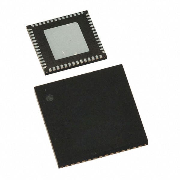
- Part No.:
- P9038-RNDGI
- Manufacturer:
- Renesas
- Category:
- Power Management - Specialized
- Package:
- 56-VFQFN Exposed Pad
- Datasheet:
-
 P9038-RNDGI.pdf
- Description:
- IC WIRELESS PWR TX
- Quantity:
- Payment:

- Shipping:

Inventory:1,577
Please send an inquiry. Send us your inquiry, and we will respond immediately.
Product details
Overview
P9038-RNDGI from Integrated Device Technology is a WPC-1.2.2-compliant wireless power transmitter IC for A5/A11 coil topologies, operating from 4.5V–6.9V input, integrating full-bridge inverter, foreign object detection (FOD), and I²C interface. It delivers up to 8W output power, supports USB D+/D− charger port detection, and operates across –40°C to +85°C in a 7 × 7 mm VFQFPN package - deployed in furniture-integrated charging pads and rugged portable electronics.
For engineers reviewing the P9038-RNDGI datasheet, P9038-RNDGI pinout, P9038-RNDGI application, or P9038-RNDGI equivalent, this page provides verified functional identity, confirmed 56-pin VFQFPN mapping, WPC-compliant demodulation capability, integrated OVP/OTP protection thresholds, and two validated alternative transmitters with documented FOD and power-stage differences.
Technical Context
The P9038-RNDGI implements a digitally controlled full-bridge inverter with cycle-by-cycle over-current protection (3–15 A programmable range) and 110–205 kHz switching frequency. Its embedded MCU executes WPC-1.2.2 communication stack, demodulates receiver packets via HPF/ISNS path, and performs real-time FOD using synchronized VSNS_AVG/ISNS_AVG sampling.
Firmware-driven GPIO configuration enables dynamic control of LED indicators, thermistor monitoring (GPIO-2), buzzer output (GPIO-4), and USB DCP detection (GPIO-5). Input over-voltage protection is resistor-programmable via OVP_SEL pin (6.3 V / 7.15 V / 7.85 V thresholds), and soft-start is configured via external RC on GATE pin.
Key Specifications
| Parameter | Value and Actual Design Meaning |
|---|---|
| Input Voltage Range | 4.5 V to 6.9 V - supports USB adapter and dedicated charger port (DCP) without external regulation |
| Max Output Power | 8 W - compliant with WPC A5/A11 coil designs when paired with P902x receivers |
| Switching Frequency | 110–205 kHz - adjustable in 12.5 ns steps for EMI optimization and coil resonance matching |
| FOD Accuracy | ±3% current sense accuracy with 10 mΩ sense resistor - meets WPC-1.2.2 foreign object detection requirements |
| OVP Thresholds | Programmable: 6.3 V (220 kΩ to GND), 7.15 V (GND), or 7.85 V (floating) - enables flexible adapter compatibility |
| Thermal Shutdown | 140°C trip / 110°C hysteresis - protects internal power stage during sustained high-load or poor heatsinking conditions |
| I²C Interface | Slave mode only after firmware load (address 0x39); supports 400 kHz max clock - used for host configuration and telemetry |
| Operating Temp | –40°C to +85°C ambient - qualified for industrial and consumer embedded environments including furniture and small appliances |
Pinout & Package
Package: 7 × 7 mm, 56-pin Very Thin Quad Flat No-Lead (VFQFPN) with exposed thermal pad (EPAD) connected to GND.
| Pin/Terminal | Circuit Role | Design Meaning |
|---|---|---|
| GND (Pins 1, 54, 56) | Signal Ground Reference | Low-impedance return for analog/digital circuits; must be tied to EPAD for thermal and noise performance |
| IN (Pins 34–37) | Main Power Input | High-current path for full-bridge inverter; requires four parallel 22 µF ceramic capacitors near pins |
| SW1/SW2 (Pins 38–41 / 30–33) | H-Bridge Switch Nodes | Drive external resonant tank; each node supports >15 A peak current with integrated gate drivers |
| BST1/BST2 (Pins 46, 25) | Bootstrap Supply Inputs | Charge high-side gate drivers; require 0.1 µF ceramic capacitor to respective SW pin |
| ISNSP_IN / ISNSN_IN (Pins 50, 49) | Differential Current Sense Inputs | Accept Kelvin connection to 10 mΩ shunt; enable precise FOD and OCP with ±3% accuracy |
| HPF (Pin 52) | Demodulator High-Pass Filter Input | Receives modulated signal from receiver coil; shielded routing with SHIELD1/SHIELD2 required for robust packet decoding |
| SCL/SDA (Pins 10, 11) | I²C Bus Interface | Post-firmware-load slave-only interface (0x39); supports host read/write of telemetry and configuration registers |
| GPIO[0:6] (Pins 3–9) | Configurable Digital I/O | Factory-configured: GPIO-2 = thermistor ADC input; GPIO-4 = 2 kHz buzzer driver; GPIO-5 = DCP detection flag |
Key Features
| Feature | Design Value |
|---|---|
| Integrated Full-Bridge Inverter | Eliminates need for 4 external MOSFETs and gate drivers - reduces BOM count and PCB area by >30% vs discrete solutions |
| WPC-1.2.2 Compliant Demodulation | On-chip analog front-end (HPF + ISNS path) and firmware stack decode receiver packets without external ICs |
| Programmable Foreign Object Detection | Uses synchronized voltage/current sampling and MCU-based algorithm to meet Qi FOD Class 0/1 requirements |
| No External EMI Filter Required | Controlled slew-rate switching and optimized layout reduce conducted/radiated emissions below WPC limits |
| Mandatory External EEPROM Support | I²C master bootload (0x52) ensures field-upgradable firmware - required for WPC certification compliance |
| USB D+/D− Charger Port Detection | Hardware-level BC 1.2 detection outputs logic-high on GPIO-5 when DCP is identified - enables adaptive power policy |
Applications
| Furniture-Integrated Charging Surfaces | PC Peripherals with Wireless Charging |
|---|---|
|
Use Scenario: Embedded in desks, nightstands, or conference tables to deliver contactless power to smartphones and earbuds. IC Role / Device Role / Timing Role: Primary transmitter controller executing WPC handshake, power negotiation, and real-time FOD monitoring. Use Value: Enables seamless user experience with no visible connectors; 8W output supports fast charging of modern devices within 3.7 mm spacing. |
Use Scenario: Integrated into wireless keyboards, mice, or docking stations requiring simultaneous data and power delivery. IC Role / Device Role / Timing Role: Manages coil excitation, demodulates receiver status packets, and coordinates with USB DP/DM detection logic. Use Value: Eliminates battery replacement; leverages existing USB power rail (4.5–6.9 V) without additional DC/DC conversion. |
| Rugged Portable Electronics | Small Appliances with Embedded Charging |
|
Use Scenario: Used in handheld test equipment, barcode scanners, or industrial tablets needing reliable charging in harsh environments. IC Role / Device Role / Timing Role: Provides fault-resilient power transfer with over-temperature shutdown (140°C), OVP, and cycle-by-cycle OCP. Use Value: Maintains operation across –40°C to +85°C ambient; GPIO-2 thermistor interface enables system-level thermal derating. |
Use Scenario: Built into kitchen appliances (e.g., cordless blenders, smart scales) where sealed enclosures prevent wired charging. IC Role / Device Role / Timing Role: Controls resonant power transfer while managing LED indicators (GPIO-3/GPIO-6) and optional buzzer feedback (GPIO-4). Use Value: Supports dual-LED status indication per WPC spec; buzzer provides audible confirmation of power transfer start/completion. |
Equivalent & Alternatives
The following parts are listed as comparable options for similar wireless power transmitter applications.
| Alternative Part | Technical Difference | Application Difference | Selection Advice |
|---|---|---|---|
| MP-A20 (MPS) | Lacks integrated demodulator; requires external comparator and ADC for FOD; 5 V only input; no USB DP/DM detection | Targeted at cost-sensitive, fixed-coil A11 systems without charger port awareness or firmware-upgrade requirement | Choose MP-A20 only if external component count and WPC certification scope are secondary to BOM cost reduction. |
| bq500212A (TI) | Supports only A11 coils; no A5 compatibility; uses proprietary FOD algorithm; 4.2–6.2 V input range; no GPIO-5 DCP flag output | Designed for single-coil, low-power (<5 W) consumer accessories where USB port type differentiation is unnecessary | Select bq500212A when targeting legacy Qi 1.1.2 systems with strict size constraints and no need for multi-coil flexibility. |
Compared with MP-A20 and bq500212A, the P9038-RNDGI uniquely integrates full WPC-1.2.2 demodulation, A5/A11 coil support, programmable OVP, and USB DCP detection - enabling certified 8W charging in compact, thermally constrained, and adapter-diverse applications without external signal conditioning.
Availability
P9038-RNDGI is available at Aetrix Electronics and suitable for furniture-integrated charging surfaces, rugged portable electronics, and small appliances requiring stable component supply, WPC-1.2.2 certification readiness, and industrial temperature operation.
Supply support for P9038-RNDGI includes scheduled delivery planning, volume procurement assistance, BOM continuity management, traceable sourcing, and lifecycle availability coordination for OEM customers, industrial embedded developers, connected-device designers, and electronics production programs.
Manufacturer
Integrated Device Technology (IDT), now part of Renesas Electronics, designs high-performance timing, memory interface, and wireless power solutions for communications, computing, and industrial markets.
The P9038-RNDGI belongs to IDT's Qi-compliant wireless power transmitter product line, engineered specifically to reduce system complexity and accelerate WPC certification for A5/A11 coil-based charging platforms.
FAQ
What is the function of the OVP_SEL pin on the P9038-RNDGI?
The OVP_SEL pin on the P9038-RNDGI selects the VBUS over-voltage protection threshold: grounded → 7.15 V, floating → 7.85 V, or pulled to GND via 220 kΩ → 6.3 V. This resistor-programmable feature allows system designers to match the P9038-RNDGI to varying input adapter specifications without changing firmware or layout. The P9038-RNDGI monitors VBUS_SNS and disables the gate driver upon threshold violation.
Does the P9038-RNDGI require an external EEPROM, and why?
Yes, the P9038-RNDGI mandates an external EEPROM pre-programmed with WPC-compliant firmware. During power-on, the P9038-RNDGI acts as I²C master (address 0x52) to load firmware before transitioning to slave mode (address 0x39). Without this EEPROM, the P9038-RNDGI falls back to internal ROM - which lacks full WPC-1.2.2 packet handling and FOD compliance. Thus, external EEPROM is essential for certified operation of the P9038-RNDGI.
How does the P9038-RNDGI implement foreign object detection (FOD)?
The P9038-RNDGI implements hardware-assisted FOD by synchronously sampling input voltage (via VSNS_AVG) and current (via ISNS_AVG) using its internal 12-bit ADC, then applying firmware-based power calculation and anomaly detection per WPC-1.2.2 Class 0/1 requirements. It requires a 10 mΩ, 1% shunt resistor and external RC filters on ISNS_AVG/VSNS_AVG to ensure time-aligned measurements. This integrated approach eliminates need for external comparators or dedicated FOD ICs in the P9038-RNDGI design.
Can the P9038-RNDGI operate with both A5 and A11 coil configurations?
Yes, the P9038-RNDGI is explicitly designed for WPC-1.2.2 compliance with both A5 (multi-coil array) and A11 (single circular coil) topologies. Its full-bridge inverter, programmable switching frequency (110–205 kHz), and adaptive demodulation engine automatically adjust to coil geometry and coupling conditions. Reference designs confirm 8W transfer with A11 coils and spatial freedom with A5 arrays - making the P9038-RNDGI suitable for both free-positioning and magnetically guided charging systems.
What GPIO pins on the P9038-RNDGI are used for USB D+/D− detection and thermal monitoring?
GPIO-5 on the P9038-RNDGI outputs a logic-high signal when USB D+/D− detection identifies a dedicated charging port (DCP), per BC 1.2 specification. GPIO-2 serves as an analog input for an external NTC thermistor, enabling system-level over-temperature monitoring and thermal derating. Both functions are enabled by default firmware and require no host intervention - providing immediate value in PC peripherals and rugged electronics using the P9038-RNDGI.
P9038-RNDGI Specifications
- Product attributes
- Attribute value
- Manufacturer:
- Renesas
- Series:
- -
- Package/Case:
- 56-VFQFN Exposed Pad
- Packaging:
- Tray
- Product Status:
- Obsolete
- Applications:
- Wireless Power Transmitter
- Current - Supply:
- -
- Voltage - Supply:
- 4.5V ~ 6.9V
- Operating Temperature:
- -40°C ~ 85°C
- Grade:
- -
- Qualification:
- -
- Mounting Type:
- Surface Mount
- Supplier Device Package:
- 56-VFQFPN (7x7)
P9038-RNDGI FAQ
1.How can I place an order for P9038-RNDGI through Aetrix?
Please submit a Request for Quotation (RFQ) for P9038-RNDGI on Aetrix. Our sales agent will provide a competitive quotation and guide you through the order confirmation once you accept the terms.
2.Are the price and stock information for P9038-RNDGI reliable?
The price and inventory of P9038-RNDGI are updated periodically and may fluctuate due to market conditions. Stock and pricing data are typically refreshed every 24 hours. Quotation validity for P9038-RNDGI is usually 5 days.
3.What payment methods are accepted for P9038-RNDGI?
We accept Wire Transfer, PayPal, Credit Card, Western Union, MoneyGram, and Escrow for P9038-RNDGI transactions.
Note: Certain payment methods may incur a processing fee.
4.How is shipping managed for P9038-RNDGI?
P9038-RNDGI orders can be shipped via leading logistics carriers, including DHL, UPS, FedEx, TNT, or Registered Mail.
Once your P9038-RNDGI order is processed, you will receive an email with the shipment details and tracking number.
Note: Tracking information may take up to 24 hours to appear. Express delivery typically takes 3–5 business days.
5.How can I obtain technical support or documentation for P9038-RNDGI?
For technical support, including P9038-RNDGI datasheets, pinout diagrams, or application guidance, please contact our engineering support team. They can provide detailed documentation and assistance for your P9038-RNDGI requirements.
6.How does Aetrix verify that P9038-RNDGI is sourced from the original manufacturer or authorized distributors?
All P9038-RNDGI products on Aetrix are procured from qualified distributors and authorized channels. Our dedicated quality assurance team conducts strict verification, including traceability checks and, if necessary, third-party testing. This ensures that P9038-RNDGI meets industry standards.
7.What is the process for return or replacement of P9038-RNDGI?
All P9038-RNDGI units undergo pre-shipment inspection (PSI). If there is an issue with P9038-RNDGI, returns or replacements are accepted under the following conditions:
1.Quantity discrepancies, incorrect items, or visible external defects (such as breakage or corrosion), acknowledged by Aetrix.
2.The issue is reported within 90 days of delivery.
3.The P9038-RNDGI part is unused and in its original packaging.
Return procedure for P9038-RNDGI:
1.Submit a request within 90 days.
2.Obtain a Return Material Authorization (RMA) from Aetrix.
P9038-RNDGI Tags

-
TPS2511DGNR
Texas Instruments

-
UTC2000/MG
Microchip Technology

-
TUSB320HAIRWBR
Texas Instruments

-
TPS61252DSGR
Texas Instruments

-
PI5USB30216CXUAEX
Diodes Incorporated

-
SN6501DBVR
Texas Instruments

-
CYPD3177-24LQXQT
Infineon Technologies
-
SN6501QDBVRQ1
Texas Instruments

-
STUSB1600AQTR
STMicroelectronics

-
SN6505BDBVR
Texas Instruments
-
SN6501DBVT
Texas Instruments

-
TPS65150PWPR
Texas Instruments
Tech Hub

TTL and CMOS logic families differ in thresholds, loading, output drive, power and timing. This engineering guide compares 74HC and 74HCT, calculates noise margins and checks 3.3 V/5 V compatibility.

A practical engineering guide to 3.3V and 5V logic compatibility, input thresholds, resistor dividers, translator ICs, MOSFET level shifting, I2C pull-ups, timing limits and power-sequencing risks.

The 74HC595 uses push-pull logic outputs, while the TPIC6B595 uses 50 V open-drain DMOS sinks for higher-power loads. This guide compares timing, current limits, 3.3 V interfacing, load wiring, thermal…

The 74HC595 converts serial data into eight stable parallel outputs. This guide covers pin functions, shift and storage timing, OE and MR behavior, drive-current limits, cascading, voltage compatibilit…

A technical comparison of level-sensitive latches and edge-triggered flip-flops, covering timing windows, setup and hold limits, master–slave operation, time borrowing, race-through, HDL inference and…

A D latch stores one bit while Enable controls when data can pass. This reference covers gate-level operation, truth tables, transparency, setup and hold timing, LE versus OE, common ICs and practical …

An SR latch stores one bit through cross-coupled feedback. This engineering reference covers NOR and NAND implementations, truth tables, forbidden-state recovery, gated operation, switch debouncing, fa…

Latch circuits retain one bit through feedback. This technical reference covers SR and D latches, truth tables, transparency, timing limits, latch-versus-flip-flop behavior, applications and common log…

An engineering guide to LED driver operation, constant-current and constant-voltage outputs, linear and switching topologies, dimming, IC selection, calculations, replacement compatibility, and fault c…

Operational amplifier guide covering op amp basics, feedback, ideal vs real op amps, common configurations, buffer circuits, offset, bias current, gain-bandwidth, slew rate, rail-to-rail limits and sel…


