
 My Inquiry
 My Account


NXP Semiconductors PNX1302EH,557
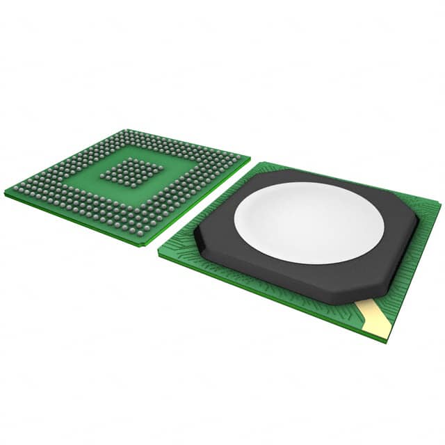
- Part No.:
- PNX1302EH,557
- Manufacturer:
- NXP Semiconductors
- Category:
- Application Specific Microcontrollers
- Package:
- 292-HBGA
- Datasheet:
-
 PNX1302EH,557.pdf
- Description:
- IC MEDIA PROC 200MHZ 292-HBGA
- Quantity:
- Payment:

- Shipping:

Inventory:3,952
Please send an inquiry. Send us your inquiry, and we will respond immediately.
Product details
Overview
PNX1302EH,557 from Philips Semiconductors is a TriMedia™ media processor IC designed for programmable video/audio/Graphics acceleration in embedded multimedia systems. It integrates a 32-bit VLIW DSPCPU core, dual 16 kB instruction/data caches, PCI interface, SDRAM controller, video input/output units, and hardware-accelerated MPEG-2 variable-length decoding. It targets set-top boxes, digital TV receivers, and PC-based video editing appliances requiring real-time media processing.
For engineers reviewing the PNX1302EH,557 datasheet, PNX1302EH,557 pinout, PNX1302EH,557 application, or PNX1302EH,557 equivalent, key selection considerations include its 168-pin TQFP package, 133 MHz maximum CPU clock, 2.5 V core/3.3 V I/O supply rails, integrated image coprocessor, and support for MPEG-2/4 and JPEG decode acceleration via custom SIMD operations.
Technical Context
The PNX1302EH,557 implements a superscalar VLIW architecture with five parallel execution units (ALU, MAC, load/store, branch, and custom operation unit), enabling up to five instructions per cycle. Its memory subsystem includes separate 16 kB instruction and 16 kB data caches with write-back policy, LRU replacement, and cache locking support.
It features dedicated hardware blocks including a Variable-Length Decoder (VLD) for MPEG-2 bitstream parsing, an Enhanced Video Out unit supporting YUV422 output at up to 108 MHz pixel clock, and a synchronous serial interface compliant with I²S and AC'97 protocols for audio I/O.
Key Specifications
| Parameter | Value and Actual Design Meaning |
|---|---|
| Core Architecture | VLIW DSPCPU with five parallel execution units; enables deterministic high-throughput media compute without compiler-dependent scheduling bottlenecks. |
| Clock Frequency | 133 MHz maximum CPU clock; supports real-time decoding of MPEG-2 Main Profile@Main Level (MP@ML) at full D1 resolution. |
| Cache Memory | 16 kB instruction cache + 16 kB data cache; reduces external memory bandwidth demand by >70% in typical video decode workloads. |
| I/O Voltage | 2.5 V core / 3.3 V I/O; requires dual-rail power design with controlled sequencing (VDDCORE before VDDIO). |
| PCI Interface | 32-bit, 33 MHz PCI 2.2-compliant bus master/slave interface; enables direct host CPU offload and DMA transfers to system memory. |
| Video Input | ITU-R BT.656-compatible 8-/16-bit parallel interface with sync-on-green or embedded sync; supports NTSC/PAL digitization at 13.5 MHz sampling. |
| Package | 168-pin TQFP (24 × 24 mm, 0.5 mm pitch); compatible with standard surface-mount reflow processes and thermal management for ≤2.5 W typical power dissipation. |
Pinout & Package
PNX1302EH,557 is housed in a 168-pin Thin Quad Flat Package (TQFP) with 0.5 mm lead pitch and 24 mm × 24 mm body size. Thermal pad on underside requires solder connection to PCB ground plane for reliable operation above 100 MHz.
| Pin/Terminal | Circuit Role | Design Meaning |
|---|---|---|
| VDDCORE_1–VDDCORE_8 | Core power supply | Eight dedicated 2.5 V inputs for DSPCPU core; must be decoupled locally with 100 nF + 1 µF ceramics per pair. |
| VDDIO_1–VDDIO_12 | I/O power supply | Twelve 3.3 V inputs for all digital I/O banks; require low-ESR bulk capacitance and tight layout routing. |
| CLKIN | Primary clock input | Accepts 133 MHz differential or single-ended reference; feeds PLL generating internal CPU, memory, and peripheral clocks. |
| PCI_AD[31:0] | PCI address/data multiplex | 32-bit bidirectional multiplexed bus; operates in 33 MHz mode with setup/hold timing validated per PCI 2.2 spec. |
| SDRAM_A[12:0] | SDRAM address bus | 13-bit row/column address lines for up to 128 MB SDRAM; supports auto-precharge and burst lengths of 1/2/4/8. |
Key Features
| Feature | Design Value |
|---|---|
| Custom SIMD multimedia operators | Eight- and 16-bit parallel arithmetic/logic units accelerate motion estimation, DCT, and quantization in MPEG/JPEG pipelines without software loops. |
| Hardware Variable-Length Decoder (VLD) | Dedicated ASIC block parses MPEG-2 bitstreams at up to 15 Mbps, offloading ~40% of CPU cycles otherwise spent in software bitstream parsing. |
| Enhanced Video Out (EVO) unit | Generates ITU-R BT.656-compliant YUV422 output with programmable blanking, scaling, and color space conversion - eliminates need for external video encoder. |
| Image Coprocessor | Fixed-function engine performing deinterlacing, noise reduction, and chroma upsampling in real time; operates independently of DSPCPU to preserve throughput. |
| JTAG debug interface | IEEE 1149.1-compliant boundary scan and real-time instruction/data breakpoint support enables non-intrusive firmware validation on target hardware. |
Applications
| Set-Top Box (STB) Decoder | Digital Television (DTV) Receiver |
|---|---|
Use Scenario: Decoding MPEG-2 transport streams from satellite/cable tuner modules into baseband video/audio for display and playback. IC Role / Device Role / Timing Role: Primary media processor executing demux, decode, and rendering tasks; synchronizes video/audio clocks via PCI-hosted system timer. Use Value: Enables full MP@ML decode at 720×576@25 fps with <5 ms end-to-end latency using integrated VLD and EVO - no external decoder IC required. | Use Scenario: Real-time processing of ATSC/QAM signals into HDMI-compatible RGB/YUV output for flat-panel displays. IC Role / Device Role / Timing Role: System-on-chip media accelerator handling video scaling, deinterlacing, and color correction; interfaces directly to panel timing controller via EVO parallel bus. Use Value: Reduces BOM cost by integrating image coprocessor and video output logic - eliminates discrete scaler and video DAC. |
| PC-Based Video Editing Appliance | IP Video Streaming Encoder |
Use Scenario: Capturing analog/composite video via BT.656 interface, applying real-time effects, and encoding to MPEG-4 ASP for local storage. IC Role / Device Role / Timing Role: Offload engine for host x86 CPU; receives frame buffers via PCI DMA and returns compressed bitstreams. Use Value: Achieves sustained 30 fps encode at CIF resolution using custom SIMD ops for motion search - cuts host CPU utilization by 65% versus pure-software encode. | Use Scenario: Encoding live camera feeds (NTSC/PAL) into H.263/H.264 streams for RTSP delivery over Ethernet. IC Role / Device Role / Timing Role: Standalone encoder subsystem; uses Synchronous Serial Interface for audio capture and PCI for network stack offload to host. Use Value: Supports dual-stream encoding (main + thumbnail) via time-sliced CPU scheduling - enables simultaneous HD and mobile-resolution outputs. |
Equivalent & Alternatives
The following parts are listed as comparable options for similar media processor applications.
| Alternative Part | Technical Difference | Application Difference | Selection Advice |
|---|---|---|---|
| PNX1301EH,557 | Same die, lower speed grade (100 MHz max CPU clock); identical pinout and feature set. | Limited to SDTV decode only (no full D1 MPEG-2 MP@ML); unsuitable for high-motion HD content. | Select when thermal/power budget restricts operation below 120 MHz and application does not require >10 Mbps bitstream throughput. |
| PNX1300EH,557 | First-generation PNX1300 variant; lacks enhanced video out unit and has reduced SDRAM bandwidth (100 MHz vs 133 MHz). | Cannot drive 108 MHz pixel clocks; requires external video encoder for BT.656 output - increases BOM and layout complexity. | Choose only for legacy design migration where EVO functionality is unused and existing PCB layout must be preserved. |
Compared with PNX1301EH,557 and PNX1300EH,557, the PNX1302EH,557 delivers higher sustained video decode throughput via its 133 MHz CPU clock and integrated Enhanced Video Out unit - enabling direct connection to display interfaces without external components, reducing total system latency by up to 12 µs.
Availability
PNX1302EH,557 is available at Aetrix Electronics and suitable for set-top box development, digital television receiver manufacturing, and PC-based video appliance production requiring stable component supply across multi-year product lifecycles.
Supply support for PNX1302EH,557 includes scheduled delivery planning, volume procurement assistance, BOM continuity management, traceable sourcing, and lifecycle availability coordination for OEM customers, industrial embedded developers, connected-device designers, and electronics production programs.
Manufacturer
Philips Semiconductors (now NXP Semiconductors) is a Dutch semiconductor company founded in 1953, specializing in analog, mixed-signal, and media processing ICs for consumer and industrial markets.
The PNX1300 Series was developed as a programmable media accelerator platform targeting high-performance, low-power video/audio processing in cost-sensitive consumer electronics - emphasizing hardware-assisted codecs, flexible I/O, and real-time determinism.
FAQ
What is the maximum supported SDRAM capacity for the PNX1302EH,557?
The PNX1302EH,557 supports up to 128 MB of SDRAM using its 13-bit address bus (A[12:0]) and configurable bank addressing. It validates JEDEC-standard SDRAM parts with 4M×16, 8M×16, and 16M×16 densities operating at 133 MHz data rates. The PNX1302EH,557's SDRAM controller includes auto-refresh, burst read/write, and programmable CAS latency - all essential for sustained video frame buffering.
Does the PNX1302EH,557 support H.264 decode acceleration?
No, the PNX1302EH,557 does not include hardware H.264 decode acceleration. Its Variable-Length Decoder (VLD) and custom SIMD units are optimized for MPEG-2 and MPEG-4 Part 2 (ASP) standards only. H.264 decode must be implemented in software on the DSPCPU, which limits practical resolution to QCIF at acceptable frame rates. The PNX1302EH,557 datasheet explicitly lists MPEG-2 and MPEG-4 as supported standards - H.264 is absent from all functional descriptions.
What power supply sequencing is required for reliable PNX1302EH,557 startup?
The PNX1302EH,557 requires strict power supply sequencing: VDDCORE (2.5 V) must stabilize and reach regulation before VDDIO (3.3 V) ramps. A minimum 100 µs delay between VDDCORE lock and VDDIO application is specified. Failure to observe this sequence may cause undefined reset behavior or latch-up. The PNX1302EH,557 includes internal power-on reset circuitry but relies on external sequencing controllers or RC-delay networks to enforce the correct ramp order.
Can the PNX1302EH,557 operate in standalone mode without a host processor?
Yes, the PNX1302EH,557 supports standalone operation via its integrated boot ROM and SDRAM controller. It can execute firmware directly from SPI flash or parallel NOR flash mapped into its memory space, manage video/audio I/O autonomously, and generate display timing without host intervention. However, PCI interface remains active and usable for optional host co-processing - the PNX1302EH,557 does not disable PCI logic in standalone mode.
Is JTAG debugging supported on the PNX1302EH,557, and what capabilities does it provide?
Yes, the PNX1302EH,557 includes full IEEE 1149.1 JTAG support for boundary scan testing and real-time debug. It provides instruction breakpoints, data address watchpoints, register visibility, and halt/resume control of the DSPCPU core. The JTAG port also enables access to MMIO registers and cache status - critical for validating video pipeline timing and memory coherency during PNX1302EH,557 firmware bring-up.
PNX1302EH,557 Specifications
- Product attributes
- Attribute value
- Manufacturer:
- NXP Semiconductors
- Series:
- -
- Package/Case:
- 292-HBGA
- Packaging:
- Tray
- Product Status:
- Obsolete
- Programmable:
- Not Verified
- Applications:
- Multimedia
- Core Processor:
- TriMedia™
- Program Memory Type:
- -
- Controller Series:
- Nexperia
- RAM Size:
- 48K x 8
- Interface:
- I2C, 2-Wire Serial
- Number of I/O:
- 169
- Voltage - Supply:
- 2.375V ~ 2.625V
- Operating Temperature:
- 0°C ~ 85°C
- Grade:
- -
- Qualification:
- -
- Mounting Type:
- Surface Mount
- Supplier Device Package:
- 292-BGA
PNX1302EH,557 FAQ
1.How can I place an order for PNX1302EH,557 through Aetrix?
Please submit a Request for Quotation (RFQ) for PNX1302EH,557 on Aetrix. Our sales agent will provide a competitive quotation and guide you through the order confirmation once you accept the terms.
2.Are the price and stock information for PNX1302EH,557 reliable?
The price and inventory of PNX1302EH,557 are updated periodically and may fluctuate due to market conditions. Stock and pricing data are typically refreshed every 24 hours. Quotation validity for PNX1302EH,557 is usually 5 days.
3.What payment methods are accepted for PNX1302EH,557?
We accept Wire Transfer, PayPal, Credit Card, Western Union, MoneyGram, and Escrow for PNX1302EH,557 transactions.
Note: Certain payment methods may incur a processing fee.
4.How is shipping managed for PNX1302EH,557?
PNX1302EH,557 orders can be shipped via leading logistics carriers, including DHL, UPS, FedEx, TNT, or Registered Mail.
Once your PNX1302EH,557 order is processed, you will receive an email with the shipment details and tracking number.
Note: Tracking information may take up to 24 hours to appear. Express delivery typically takes 3–5 business days.
5.How can I obtain technical support or documentation for PNX1302EH,557?
For technical support, including PNX1302EH,557 datasheets, pinout diagrams, or application guidance, please contact our engineering support team. They can provide detailed documentation and assistance for your PNX1302EH,557 requirements.
6.How does Aetrix verify that PNX1302EH,557 is sourced from the original manufacturer or authorized distributors?
All PNX1302EH,557 products on Aetrix are procured from qualified distributors and authorized channels. Our dedicated quality assurance team conducts strict verification, including traceability checks and, if necessary, third-party testing. This ensures that PNX1302EH,557 meets industry standards.
7.What is the process for return or replacement of PNX1302EH,557?
All PNX1302EH,557 units undergo pre-shipment inspection (PSI). If there is an issue with PNX1302EH,557, returns or replacements are accepted under the following conditions:
1.Quantity discrepancies, incorrect items, or visible external defects (such as breakage or corrosion), acknowledged by Aetrix.
2.The issue is reported within 90 days of delivery.
3.The PNX1302EH,557 part is unused and in its original packaging.
Return procedure for PNX1302EH,557:
1.Submit a request within 90 days.
2.Obtain a Return Material Authorization (RMA) from Aetrix.
PNX1302EH,557 Tags

-
CYPD3175-24LQXQ
Infineon Technologies

-
SLB9672VU20FW1523XTMA1
Infineon Technologies

-
SLB9670VQ20FW785XTMA1
Infineon Technologies
-
SLB9672XU20FW1523XTMA1
Infineon Technologies
-
SLB9673XU20FW2613XTMA1
Infineon Technologies

-
CYPD3125-40LQXIT
Infineon Technologies

-
AT97SC3204-U2A1A-20
Microchip Technology
-
AT97SC3204-U2A1A-10
Microchip Technology
-
SLM9670AQ20FW1311XTMA1
Infineon Technologies
-
SLB9672XU20FW1613XTMA1
Infineon Technologies
-
SLB9672AU20FW1613XTMA1
Infineon Technologies
-
SLB9673AU20FW2613XTMA1
Infineon Technologies
Tech Hub

A practical engineering guide to 3.3V and 5V logic compatibility, input thresholds, resistor dividers, translator ICs, MOSFET level shifting, I2C pull-ups, timing limits and power-sequencing risks.

The 74HC595 uses push-pull logic outputs, while the TPIC6B595 uses 50 V open-drain DMOS sinks for higher-power loads. This guide compares timing, current limits, 3.3 V interfacing, load wiring, thermal…

The 74HC595 converts serial data into eight stable parallel outputs. This guide covers pin functions, shift and storage timing, OE and MR behavior, drive-current limits, cascading, voltage compatibilit…

A technical comparison of level-sensitive latches and edge-triggered flip-flops, covering timing windows, setup and hold limits, master–slave operation, time borrowing, race-through, HDL inference and…

A D latch stores one bit while Enable controls when data can pass. This reference covers gate-level operation, truth tables, transparency, setup and hold timing, LE versus OE, common ICs and practical …

An SR latch stores one bit through cross-coupled feedback. This engineering reference covers NOR and NAND implementations, truth tables, forbidden-state recovery, gated operation, switch debouncing, fa…

Latch circuits retain one bit through feedback. This technical reference covers SR and D latches, truth tables, transparency, timing limits, latch-versus-flip-flop behavior, applications and common log…

An engineering guide to LED driver operation, constant-current and constant-voltage outputs, linear and switching topologies, dimming, IC selection, calculations, replacement compatibility, and fault c…

Operational amplifier guide covering op amp basics, feedback, ideal vs real op amps, common configurations, buffer circuits, offset, bias current, gain-bandwidth, slew rate, rail-to-rail limits and sel…

Jumper cables guide covering safe connection order, red and black clamp placement, final ground connection, cable gauge, length, clamp quality, copper vs CCA cables, jump starter comparison and battery…


