
 My Inquiry
 My Account


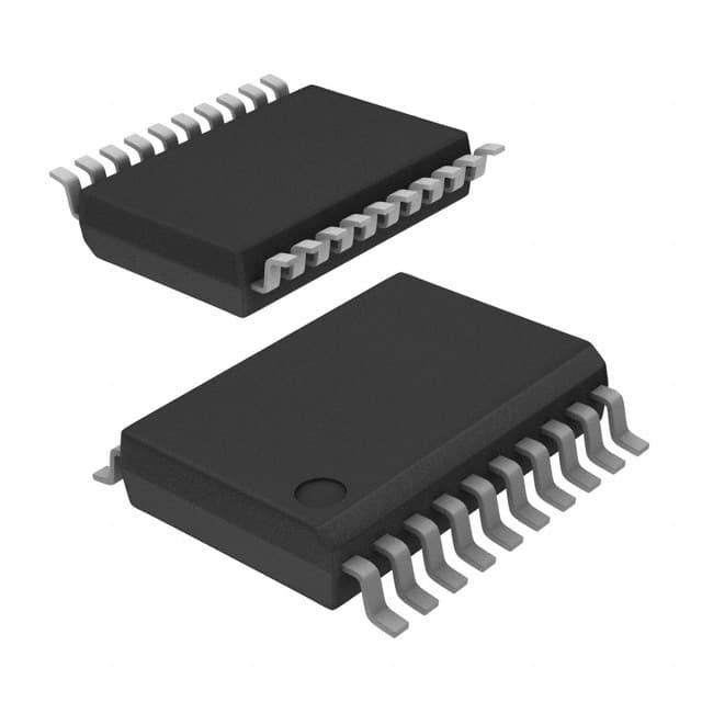
Microchip Technology RFPIC12F675H-I/SS
- Part No.:
- RFPIC12F675H-I/SS
- Manufacturer:
- Microchip Technology
- Category:
- Application Specific Microcontrollers
- Package:
- 20-SSOP (0.209", 5.30mm Width)
- Datasheet:
-
 RFPIC12F675H-I/SS.pdf
- Description:
- IC MCU 1KX14 RF FSK/ASK 20SSOP
- Quantity:
- Payment:

- Shipping:

Inventory:1,962
Please send an inquiry. Send us your inquiry, and we will respond immediately.
Product details
Overview
RFPIC12F675H-I/SS from Microchip Technology is a FLASH-based 8-bit RISC microcontroller with integrated UHF ASK/FSK transmitter, operating in the 850–930 MHz band. It features 1024 × 14 words of FLASH, 128 bytes of EEPROM, 10-bit ADC (4 channels), dual timers (Timer0/Timer1), analog comparator with 16 reference levels, and 6 programmable I/O pins - enabling compact wireless sensor nodes such as tire pressure monitors and garage door openers.
For engineers reviewing the RFPIC12F675H-I/SS datasheet, RFPIC12F675H-I/SS pinout, RFPIC12F675H-I/SS application, or RFPIC12F675H-I/SS equivalent, key selection criteria include its integrated RF transmitter architecture (VCO + loop filter + PA), REFCLK/8 output for H-band operation, 20-pin SSOP package, FCC Part 15.231/EN 300 220 compliance, and low-power SLEEP mode (0.1 µA standby).
Technical Context
The RFPIC12F675H-I/SS integrates a PICmicro® Mid-Range CPU core with an on-die UHF transmitter subsystem. Its RF section uses a crystal oscillator multiplied by 32 to generate carrier frequency, with phase-locked VCO and integrated power amplifier delivering +10 dBm to –12 dBm output in four discrete steps. The REFCLK output is divided by 8 (specific to H-band variant), supporting narrowband receiver synchronization.
Peripheral integration includes Timer1 with gate control and LP oscillator support for wake-up timing, 10-bit ADC with selectable voltage reference, and interrupt-on-change capability across all six GPIOs. Memory architecture supports in-circuit serial programming (ICSP™) via GP0/GP1, with 100,000 FLASH write endurance and >40-year data retention.
Key Specifications
| Parameter | Value and Actual Design Meaning |
|---|---|
| Operating Frequency Band | 850–930 MHz - defines regulatory compliance scope (FCC Part 15.231, EN 300 220) and antenna matching requirements. |
| Transmitter Output Power | +10 dBm to –12 dBm in 4 steps - enables range/power trade-off tuning without external PA bias adjustment. |
| REFCLK Output Division | ÷8 - specific to RFPIC12F675H variant; provides stable reference for external narrowband receivers. |
| ADC Resolution & Channels | 10-bit, 4-channel - supports precision analog sensing (e.g., pressure, temperature) with internal VREF or external reference. |
| SLEEP Current | 0.1 µA standby - enables multi-year battery life in intermittent transmission applications like TPMS. |
| FLASH Endurance | 100,000 write cycles - supports field firmware updates in deployed wireless endpoints. |
| EEPROM Retention | >40 years - ensures long-term storage of calibration data or device identity without refresh. |
Pinout & Package
Package: 20-pin SSOP (Small Outline Package), 0.65 mm pitch, body width 5.3 mm - compatible with standard surface-mount reflow processes and space-constrained PCB layouts.
| Pin/Terminal | Circuit Role | Design Meaning |
|---|---|---|
| VDD / VSS | Digital power supply / ground | Separate digital rail; decoupling required near VDD pin to suppress switching noise coupling into RF section. |
| VDDRF / VSSRF (×2) | RF power supply / RF ground | Dedicated RF supply path isolates analog/RF domains; dual VSSRF pins reduce ground impedance for PA output stage. |
| RFXTAL | Crystal input for RF oscillator | Connects to fundamental-mode quartz crystal; frequency determines final carrier (×32 multiplication). |
| ANT | RF power amplifier output | Direct connection to matching network/antenna; requires 50 Ω impedance control and ESD protection. |
| REFCLK | Reference clock output | ÷8 divided output (H-band specific); used for synchronizing external narrowband receivers or clocking baseband logic. |
| DATAASK / DATAFSK | Modulation data inputs | TTL-level digital baseband inputs; ASK/FSK modulation selected via internal configuration, not pin-strapped. |
| RFEN | RF enable control | Active-high signal enabling transmitter block; allows precise duty-cycle control to minimize average current draw. |
| GP0–GP5 | Programmable I/O with analog capability | 6 bidirectional pins with weak pull-ups, interrupt-on-change, and analog functions (ADC/CMP) - eliminates need for external GPIO expanders. |
Key Features
| Feature | Design Value |
|---|---|
| Integrated UHF Transmitter | Combines crystal oscillator, VCO, loop filter, and power amplifier - reduces BOM count by ≥7 passive RF components vs. discrete solutions. |
| Low-Power SLEEP Mode | 0.1 µA standby current with watchdog enabled - extends CR2032 battery life to >10 years in infrequent-transmit applications. |
| On-Chip 10-Bit ADC | 4-channel, software-selectable reference - enables direct sensor interfacing (e.g., pressure transducer, thermistor) without external ADC. |
| Interrupt-on-Change GPIO | All 6 I/O pins support edge-triggered interrupts - allows wake-up from SLEEP on external event (e.g., door contact closure) without polling. |
| In-Circuit Serial Programming | ICSP™ via GP0/GP1 - permits firmware updates after solder-down, supporting post-production calibration and field upgrades. |
Applications
| Automotive Remote Keyless Entry (RKE) | Tire Pressure Monitoring System (TPMS) |
|---|---|
|
Use Scenario: Compact fob transmitting encrypted lock/unlock commands to vehicle receiver. IC Role / Device Role / Timing Role: Primary MCU and ASK transmitter; generates Manchester-encoded payload and drives RF stage at 868/915 MHz. Use Value: Integrated RF eliminates external synthesizer and PA, reducing fob size and bill-of-materials cost while meeting automotive EMC requirements. |
Use Scenario: Battery-powered wheel-mounted sensor measuring pressure/temperature and transmitting alerts. IC Role / Device Role / Timing Role: Sensor interface MCU with ultra-low-power SLEEP and fast RF wake-up (5 µs); handles ADC sampling, data formatting, and burst transmission. Use Value: 0.1 µA standby current and integrated 10-bit ADC enable >7-year CR2032 battery life without compromising measurement resolution. |
| Garage Door Opener Transmitter | Wireless Building Access Control |
|
Use Scenario: Handheld remote sending secure rolling-code signals to motorized gate controller. IC Role / Device Role / Timing Role: Secure code generator and FSK transmitter; uses internal comparator for tamper detection and Timer1 for precise timing of code intervals. Use Value: On-chip FSK modulation with crystal pulling eliminates need for external modulator IC, simplifying layout and improving frequency stability. |
Use Scenario: Keypad or card reader node transmitting access credentials to central security panel. IC Role / Device Role / Timing Role: Low-power wireless endpoint with GPIO-driven keypad scan and RFEN-gated transmission; uses EEPROM to store unique device ID and encryption keys. Use Value: 128-byte EEPROM with 1M write endurance supports secure credential storage and firmware update logging over product lifetime. |
Equivalent & Alternatives
The following parts are listed as comparable options for similar RF microcontroller applications.
| Alternative Part | Technical Difference | Application Difference | Selection Advice |
|---|---|---|---|
| rfPIC12F675F-I/SS | 380–450 MHz band; REFCLK ÷4 output; same core/peripherals | Designed for EU 433 MHz ISM band; incompatible crystal and antenna matching for 868/915 MHz systems | Select only when targeting 433 MHz regulatory domain and existing 433 MHz receiver infrastructure. |
| rfPIC12F675K-I/SS | 290–350 MHz band; REFCLK ÷4 output; identical MCU architecture | Optimized for North American 315 MHz RKE; requires different crystal and RF front-end design | Choose for legacy 315 MHz automotive or alarm systems where FCC Part 15.231 315 MHz certification already exists. |
Compared with rfPIC12F675F-I/SS and rfPIC12F675K-I/SS, the RFPIC12F675H-I/SS provides H-band RF performance (850–930 MHz) with ÷8 REFCLK - making it the sole option for 868/915 MHz deployments requiring narrowband receiver synchronization and FCC/EN compliance in that band.
Availability
RFPIC12F675H-I/SS is available at Aetrix Electronics and suitable for automotive RKE, TPMS, garage door openers, and wireless building access systems requiring stable component supply and long-lifecycle support.
Supply support for RFPIC12F675H-I/SS includes scheduled delivery planning, volume procurement assistance, BOM continuity management, traceable sourcing, and lifecycle availability coordination for OEM customers, industrial embedded developers, connected-device designers, and electronics production programs.
Manufacturer
Microchip Technology Inc. is a leading provider of microcontroller, mixed-signal, analog, and Flash-IP solutions, headquartered in Chandler, Arizona, with global design and manufacturing operations.
The rfPIC12F675 product line was designed to integrate RF transmission capability directly into cost-sensitive, battery-operated embedded endpoints - targeting remote controls, sensors, and security peripherals where minimal external components and regulatory-certified RF performance are critical.
FAQ
What is the RF frequency range supported by the RFPIC12F675H-I/SS?
The RFPIC12F675H-I/SS operates in the 850–930 MHz band, specifically targeting the 868 MHz (EU) and 915 MHz (North America) ISM bands. Its RF section uses a crystal oscillator multiplied by 32, so a 27 MHz crystal yields 864 MHz output. This band assignment is fixed per variant and cannot be reconfigured in firmware. The RFPIC12F675H-I/SS must be paired with a crystal and matching network optimized for this range.
Does the RFPIC12F675H-I/SS support both ASK and FSK modulation?
Yes, the RFPIC12F675H-I/SS supports both ASK and FSK modulation through dedicated DATAASK and DATAFSK input pins. ASK modulation is applied directly to the RF power amplifier, while FSK is implemented by crystal pulling via the FSKOUT pin, which modulates the reference crystal's load capacitance. Both schemes operate up to 40 Kbps and comply with FCC Part 15.231 and EN 300 220 regulations when configured per Microchip's reference designs.
What is the purpose of the REFCLK pin on the RFPIC12F675H-I/SS?
The REFCLK pin on the RFPIC12F675H-I/SS outputs a divided version of the RF crystal oscillator - specifically divided by 8 for the H-band variant. This signal provides a stable, low-jitter reference for synchronizing external narrowband receivers, enabling improved interference immunity and extended communication range. Unlike the K/F variants (which output ÷4), the ÷8 division is hardwired and unique to the RFPIC12F675H-I/SS.
How many analog input channels does the RFPIC12F675H-I/SS ADC support?
The RFPIC12F675H-I/SS includes a 10-bit analog-to-digital converter with 4 configurable input channels (AN0–AN3), mapped to GP0, GP1, GP2, and GP4 respectively. Each channel supports software-selectable voltage reference (VDD, VSS, or internal 2.048 V), and conversion results are stored in ADRESH/ADRESL registers. The ADC is fully integrated - no external sample-and-hold or reference ICs are required.
Can the RFPIC12F675H-I/SS be programmed in-circuit after PCB assembly?
Yes, the RFPIC12F675H-I/SS supports In-Circuit Serial Programming (ICSP™) using GP0 (ICSPDAT) and GP1 (ICSPCLK) pins. This allows full firmware loading, verification, and calibration data programming after solder-down, eliminating the need for socketed programming. A standard 5-pin ICSP header (VDD, VSS, PGD, PGC, MCLR) is sufficient, and the process is compatible with Microchip's MPLAB® ICD and PICkit™ programmers.
RFPIC12F675H-I/SS Specifications
- Product attributes
- Attribute value
- Manufacturer:
- Microchip Technology
- Series:
- PIC®
- Package/Case:
- 20-SSOP (0.209", 5.30mm Width)
- Packaging:
- Tube
- Product Status:
- Active
- Programmable:
- Verified
- Applications:
- RKE, Security Systems
- Core Processor:
- PIC
- Program Memory Type:
- FLASH (1.75kB)
- Controller Series:
- rfPIC™
- RAM Size:
- 64 x 8
- Interface:
- -
- Number of I/O:
- 6
- Voltage - Supply:
- 2V ~ 5.5V
- Operating Temperature:
- -40°C ~ 85°C
- Grade:
- -
- Qualification:
- -
- Mounting Type:
- Surface Mount
- Supplier Device Package:
- 20-SSOP
RFPIC12F675H-I/SS FAQ
1.How can I place an order for RFPIC12F675H-I/SS through Aetrix?
Please submit a Request for Quotation (RFQ) for RFPIC12F675H-I/SS on Aetrix. Our sales agent will provide a competitive quotation and guide you through the order confirmation once you accept the terms.
2.Are the price and stock information for RFPIC12F675H-I/SS reliable?
The price and inventory of RFPIC12F675H-I/SS are updated periodically and may fluctuate due to market conditions. Stock and pricing data are typically refreshed every 24 hours. Quotation validity for RFPIC12F675H-I/SS is usually 5 days.
3.What payment methods are accepted for RFPIC12F675H-I/SS?
We accept Wire Transfer, PayPal, Credit Card, Western Union, MoneyGram, and Escrow for RFPIC12F675H-I/SS transactions.
Note: Certain payment methods may incur a processing fee.
4.How is shipping managed for RFPIC12F675H-I/SS?
RFPIC12F675H-I/SS orders can be shipped via leading logistics carriers, including DHL, UPS, FedEx, TNT, or Registered Mail.
Once your RFPIC12F675H-I/SS order is processed, you will receive an email with the shipment details and tracking number.
Note: Tracking information may take up to 24 hours to appear. Express delivery typically takes 3–5 business days.
5.How can I obtain technical support or documentation for RFPIC12F675H-I/SS?
For technical support, including RFPIC12F675H-I/SS datasheets, pinout diagrams, or application guidance, please contact our engineering support team. They can provide detailed documentation and assistance for your RFPIC12F675H-I/SS requirements.
6.How does Aetrix verify that RFPIC12F675H-I/SS is sourced from the original manufacturer or authorized distributors?
All RFPIC12F675H-I/SS products on Aetrix are procured from qualified distributors and authorized channels. Our dedicated quality assurance team conducts strict verification, including traceability checks and, if necessary, third-party testing. This ensures that RFPIC12F675H-I/SS meets industry standards.
7.What is the process for return or replacement of RFPIC12F675H-I/SS?
All RFPIC12F675H-I/SS units undergo pre-shipment inspection (PSI). If there is an issue with RFPIC12F675H-I/SS, returns or replacements are accepted under the following conditions:
1.Quantity discrepancies, incorrect items, or visible external defects (such as breakage or corrosion), acknowledged by Aetrix.
2.The issue is reported within 90 days of delivery.
3.The RFPIC12F675H-I/SS part is unused and in its original packaging.
Return procedure for RFPIC12F675H-I/SS:
1.Submit a request within 90 days.
2.Obtain a Return Material Authorization (RMA) from Aetrix.
RFPIC12F675H-I/SS Tags

-
CYPD3175-24LQXQ
Infineon Technologies

-
SLB9672VU20FW1523XTMA1
Infineon Technologies

-
SLB9670VQ20FW785XTMA1
Infineon Technologies
-
SLB9672XU20FW1523XTMA1
Infineon Technologies
-
SLB9673XU20FW2613XTMA1
Infineon Technologies

-
CYPD3125-40LQXIT
Infineon Technologies

-
AT97SC3204-U2A1A-20
Microchip Technology
-
AT97SC3204-U2A1A-10
Microchip Technology
-
SLM9670AQ20FW1311XTMA1
Infineon Technologies
-
SLB9672XU20FW1613XTMA1
Infineon Technologies
-
SLB9672AU20FW1613XTMA1
Infineon Technologies
-
SLB9673AU20FW2613XTMA1
Infineon Technologies
Tech Hub

TTL and CMOS logic families differ in thresholds, loading, output drive, power and timing. This engineering guide compares 74HC and 74HCT, calculates noise margins and checks 3.3 V/5 V compatibility.

A practical engineering guide to 3.3V and 5V logic compatibility, input thresholds, resistor dividers, translator ICs, MOSFET level shifting, I2C pull-ups, timing limits and power-sequencing risks.

The 74HC595 uses push-pull logic outputs, while the TPIC6B595 uses 50 V open-drain DMOS sinks for higher-power loads. This guide compares timing, current limits, 3.3 V interfacing, load wiring, thermal…

The 74HC595 converts serial data into eight stable parallel outputs. This guide covers pin functions, shift and storage timing, OE and MR behavior, drive-current limits, cascading, voltage compatibilit…

A technical comparison of level-sensitive latches and edge-triggered flip-flops, covering timing windows, setup and hold limits, master–slave operation, time borrowing, race-through, HDL inference and…

A D latch stores one bit while Enable controls when data can pass. This reference covers gate-level operation, truth tables, transparency, setup and hold timing, LE versus OE, common ICs and practical …

An SR latch stores one bit through cross-coupled feedback. This engineering reference covers NOR and NAND implementations, truth tables, forbidden-state recovery, gated operation, switch debouncing, fa…

Latch circuits retain one bit through feedback. This technical reference covers SR and D latches, truth tables, transparency, timing limits, latch-versus-flip-flop behavior, applications and common log…

An engineering guide to LED driver operation, constant-current and constant-voltage outputs, linear and switching topologies, dimming, IC selection, calculations, replacement compatibility, and fault c…

Operational amplifier guide covering op amp basics, feedback, ideal vs real op amps, common configurations, buffer circuits, offset, bias current, gain-bandwidth, slew rate, rail-to-rail limits and sel…


