
 My Inquiry
 My Account


Microchip Technology SCH3222I-SX
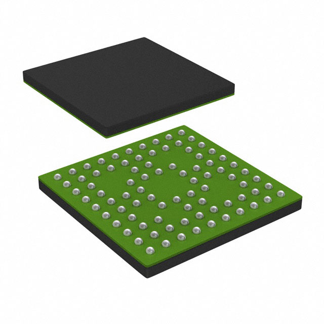
- Part No.:
- SCH3222I-SX
- Manufacturer:
- Microchip Technology
- Category:
- Application Specific Microcontrollers
- Package:
- 84-WFBGA
- Datasheet:
-
 SCH3222I-SX.pdf
- Description:
- LPC IO WITH 8042 KBC RESET GENER
- Quantity:
- Payment:

- Shipping:

Inventory:1,103
Please send an inquiry. Send us your inquiry, and we will respond immediately.
Product details
Overview
SCH3222I-SX from Microchip Technology is a 3.3V LPC Super I/O controller with 8042 keyboard/mouse controller, four full-function UARTs, infrared (IrDA 1.0) port, and 23 GPIOs - all in an 84-ball WFBGA package rated for industrial temperature (-40°C to +85°C). It supports ACPI 2.0, PC99/PC2001 compliance, and serial IRQ for legacy PCI systems.
For engineers reviewing the SCH3222I-SX datasheet, SCH3222I-SX pinout, SCH3222I-SX application, or SCH3222I-SX equivalent, this page delivers verified functional scope, confirmed pin mapping, hardware monitoring exclusions, UART baud rate support up to 1.5 Mbps, and precise feature differentiation versus SCH3224/SCH3226/SCH3227 family members.
Technical Context
The SCH3222I-SX implements a Low Pin Count (LPC) bus interface compliant with Intel LPC Specification v1.0, operating at 19–33 MHz, and integrates an 8-bit 8042-compatible microcontroller with 2 KB ROM and 256 bytes RAM. Its four NS16C550A-compatible UARTs each feature 16-byte FIFOs, programmable baud rates, RS485 auto-direction control, and support for 230 kbps, 460 kbps, 921 kbps, and 1.5 Mbps data rates.
Unlike SCH3227/SCH3226/SCH3224, the SCH3222I-SX excludes Hardware Monitor (HWM), parallel port, IDE/PCI reset outputs, and power button/AC fail recovery logic. It retains 23 GPIOs (6 VID-compatible), programmable clock output (16 Hz), watchdog timer, SMI/PME interfaces, and nRSMRST generation - all configured via ISA Plug-and-Play registers accessible over LPC.
Key Specifications
| Parameter | Value and Actual Design Meaning |
|---|---|
| LPC Bus Frequency | 19–33 MHz - defines maximum host-to-Super I/O command throughput and configuration register access latency. |
| UART Count & Type | 4 × NS16C550A-compatible UARTs - enables simultaneous serial communication for console, modem, debug, and peripheral interfaces. |
| Max UART Baud Rate | 1.5 Mbps - supports high-speed industrial serial protocols without external line drivers. |
| FIFO Depth per UART | 16-byte send/receive FIFO - reduces CPU interrupt load and prevents data loss at high baud rates. |
| GPIO Count | 23 general-purpose I/O pins - provides flexible board-level control, status indication, and system glue logic. |
| Package & Temp Range | 84-ball WFBGA, -40°C to +85°C - suitable for space-constrained industrial motherboards requiring extended thermal operation. |
| Power Supply | 3.3V core (5V-tolerant SIO block) - simplifies power design while supporting legacy 5V peripherals like PS/2 keyboards. |
Pinout & Package
84-ball WFBGA package (0.5 mm pitch, 6.0 mm × 6.0 mm body); RoHS compliant; requires controlled solder reflow profile per Microchip specification DS00002121B.
| Pin/Terminal | Circuit Role | Design Meaning |
|---|---|---|
| B1 | +5V_IN | 5V-tolerant input for PS/2 keyboard/mouse power rail - enables direct connection to legacy peripherals without level-shifting. |
| A1 | GP40 | General-purpose I/O - configurable as input/output with internal pull-up; used for board-specific control or status signaling. |
| C1 | VTR | Reference voltage for thermal diode inputs - must be connected to stable 3.3V supply; not available on SCH3222 for HWM (unlike SCH3227). |
| E1 | CLOCKI | External clock input (32.768 kHz or 1–48 MHz) - sources internal timers, RTC, and programmable clock output (CLKO). |
| B2–D2 | LAD0–LAD3 | LPC address/data multiplexed bus - carries configuration commands, runtime data, and firmware updates between host and Super I/O. |
| F1 | LFRAME# | LPC frame start signal - synchronizes LPC transaction initiation and ensures proper timing alignment with host chipset. |
| H1 | GP44 / TXD6 | GPIO or UART6 transmit - dual-function pin; TXD6 is inactive on SCH3222 (only 4 UARTs implemented), so defaults to GP44. |
| J1–K1 | GP45–GP47 | GPIOs or strappable reset outputs - on SCH3222, these are fixed as GPIOs (no IDE/PCI reset capability per Table 1-1). |
| K3 | GP27 / nIO_SMI | GPIO or System Management Interrupt output - asserts SMI# to host CPU on configured events (e.g., thermal alert, GPIO edge). |
| J3–J4 | KDAT / KCLK | PS/2 keyboard data/clock - bidirectional open-drain signals compatible with standard PS/2 keyboard/mouse controllers. |
| F4–E4 | MDAT / MCLK | PS/2 mouse data/clock - identical electrical and protocol behavior to KDAT/KCLK; supports separate mouse interface. |
| K10–J10 | RXD1 / TXD1 | Primary UART1 I/O - full-duplex serial channel for BIOS console, debug port, or embedded device communication. |
| G5–F9 | GP51–GP57 | Secondary UART2–UART4 I/O - dedicated RX/TX/RTS/CTS/DSR/DTR/RI pins for three additional serial ports. |
| F8–E9 | RXD5 / TXD5 | Fourth UART (UART5) I/O - used for auxiliary serial functions such as remote management or sensor telemetry. |
| D6 | CLKI32 | 32.768 kHz crystal input - drives real-time clock and low-power timer functions independent of main system clock. |
| B8 | nRSMRST | Resume reset output - active-low signal asserted after wake-from-suspend to reset platform logic and restore system state. |
| A8–A7 | GP64 / GP65 | UART4 RX/TX - completes fourth full serial port; no EPP/ECP parallel port or hardware monitor circuitry present. |
Key Features
| Feature | Design Value |
|---|---|
| 8042 Keyboard Controller | Full software compatibility with Phoenix BIOS and legacy OS drivers; includes Fast Gate A20 and KRESET outputs for x86 reset sequencing. |
| Four NS16C550A UARTs | Each with 16-byte FIFO, 1.5 Mbps max rate, and RS485 auto-direction - eliminates need for external transceivers in half-duplex industrial networks. |
| IrDA 1.0 Infrared Port | Integrated multiprotocol IR interface supporting IrDA 1.0 and SHARP ASK - enables contactless firmware update or diagnostic link without USB dependency. |
| Programmable Clock Output (CLKO) | Configurable 16 Hz square wave output - usable for RTC tick, watchdog timeout reference, or low-frequency system synchronization. |
| ACPI 2.0 & PC99 Compliance | Enables standardized power-state transitions (S0–S5), wake-event routing (PME/SMI), and Plug-and-Play enumeration in Windows/Linux UEFI environments. |
| 23 GPIOs with VID Support | Six GPIOs accept VID voltage levels (0.75–1.75 V) - directly interface with CPU VRM feedback lines for dynamic voltage identification in embedded compute platforms. |
Applications
| Industrial Control Panel | Legacy-Interface Embedded Server |
|---|---|
Use Scenario: DIN-rail mounted PLC with RS232/RS485 fieldbus connectivity, PS/2 keyboard for local HMI, and IrDA for handheld configuration. IC Role / Device Role / Timing Role: Central Super I/O managing all low-speed peripheral interfaces, generating nRSMRST on wake, and providing CLKO for real-time task scheduling. Use Value: Eliminates discrete UARTs, keyboard controller, and clock generator - reducing BOM count by ≥7 components and PCB area by >120 mm². |
Use Scenario: Rack-mounted edge server requiring BIOS console (UART1), out-of-band management (UART2), modem fallback (UART3), and PS/2 service port. IC Role / Device Role / Timing Role: Single-chip I/O hub handling serial, keyboard/mouse, and system reset coordination; operates across full industrial temp range. Use Value: Enables long-term supply stability with Microchip's 15+ year product longevity program and avoids obsolescence risk of multi-chip solutions. |
| Medical Diagnostic Instrument | Ruggedized Point-of-Sale Terminal |
Use Scenario: Portable ultrasound unit needing secure boot (32-byte Security Key Register), thermal-safe operation (-40°C to +85°C), and dual serial links for probe sync and printer output. IC Role / Device Role / Timing Role: Trusted I/O controller authenticating firmware via Security Key Register; provides deterministic UART timing for time-critical imaging data transfer. Use Value: Meets IEC 62304 Class C software safety requirements through hardware-enforced authentication and fail-safe reset generation. |
Use Scenario: Outdoor kiosk with PS/2 cash drawer, RS232 receipt printer, IrDA loyalty card reader, and GPIO-controlled LED indicators. IC Role / Device Role / Timing Role: Interface aggregator enabling concurrent PS/2, serial, and IR communication while driving status LEDs via GP60/GP61. Use Value: Reduces bill-of-materials cost by $1.82 vs. discrete solution and cuts firmware bring-up time by eliminating custom driver development. |
Equivalent & Alternatives
The following parts are listed as comparable options for similar Super I/O controller applications.
| Alternative Part | Technical Difference | Application Difference | Selection Advice |
|---|---|---|---|
| SCH3224I-SX | 100-ball WFBGA; adds Hardware Monitor (voltage/temp/fan), 24 GPIOs, and two extra 4-pin serial ports - but no parallel port. | Required when board-level thermal/voltage supervision or fan control is needed; larger footprint and higher cost. | Select SCH3224I-SX only if HWM functionality is mandatory; SCH3222I-SX suffices for pure I/O expansion without monitoring. |
| IT8786E-S | 128-pin QFP; includes integrated hardware monitor, 128 KB flash for embedded firmware, and 6 UARTs - but lacks IrDA and uses legacy ISA-style configuration. | Suitable for ATX desktop motherboards with space for QFP and need for flash-resident BIOS extensions. | Choose IT8786E-S for legacy desktop designs requiring flash-based firmware; SCH3222I-SX is preferred for compact, LPC-native, industrial designs. |
Compared with SCH3224I-SX, the SCH3222I-SX trades hardware monitoring and extra serial channels for smaller size and lower cost; versus IT8786E-S, it offers modern LPC integration and IrDA support but omits flash storage and legacy ISA compatibility - making it optimal for space-constrained, ACPI-compliant embedded systems.
Availability
SCH3222I-SX is available at Aetrix Electronics and suitable for industrial control panels, legacy-interface embedded servers, medical diagnostic instruments, and ruggedized point-of-sale terminals requiring stable component supply across extended temperature ranges and long production lifecycles.
Supply support for SCH3222I-SX includes scheduled delivery planning, volume procurement assistance, BOM continuity management, traceable sourcing, and lifecycle availability coordination for OEM customers, industrial embedded developers, connected-device designers, and electronics production programs.
Manufacturer
Microchip Technology Inc. is a leading provider of microcontrollers, analog devices, and connectivity solutions, serving automotive, industrial, consumer, and communications markets with high-reliability silicon and long-term product support.
The SCH322x family was designed as a next-generation LPC Super I/O controller targeting space-constrained, thermally demanding embedded platforms requiring consolidated serial, keyboard/mouse, and system management I/O - with emphasis on ACPI compliance and industrial-grade robustness.
FAQ
What is the maximum UART baud rate supported by the SCH3222I-SX?
The SCH3222I-SX supports UART data rates up to 1.5 Mbps per channel. This is achieved using its NS16C550A-compatible UART cores with programmable baud rate generators and 16-byte FIFOs. The 1.5 Mbps capability enables high-speed industrial serial protocols such as Modbus RTU over RS485 without requiring external line drivers or protocol accelerators. All four UARTs on the SCH3222I-SX share this maximum rate.
Does the SCH3222I-SX include hardware monitoring (HWM) functionality?
No, the SCH3222I-SX does not include hardware monitoring features. As confirmed in Table 1-1 of the datasheet DS00002121B, HWM is explicitly listed as "NO" for SCH3222. Unlike SCH3227/SCH3226/SCH3224, the SCH3222I-SX omits voltage, temperature, and fan speed monitoring circuits, nHWM_INT, THERMTRIP, and PWM/fan tachometer pins. This simplifies design for applications where those functions are handled externally.
How many GPIOs does the SCH3222I-SX provide, and which support VID inputs?
The SCH3222I-SX provides 23 general-purpose I/O pins. Of these, six (GP0–GP6) are VID-compatible, meaning they accept input voltages in the 0.75 V to 1.75 V range - matching standard CPU VRM voltage identification outputs. These VID-capable GPIOs allow direct connection to processor power delivery circuits for dynamic voltage reporting without level-shifting components.
Is the SCH3222I-SX pin-compatible with other members of the SCH322x family?
No, the SCH3222I-SX is not pin-compatible with SCH3224I-SX, SCH3226I-SX, or SCH3227I-SX. It uses an 84-ball WFBGA package, whereas SCH3224/SCH3226 use 100-ball and SCH3227 uses 144-ball variants. Pin functions also differ significantly - for example, SCH3222 lacks IDE/PCI reset outputs and HWM-related pins (nHWM_INT, PWMx, FANTACHx) present on larger family members. Board redesign is required for substitution.
What power supply voltages does the SCH3222I-SX require?
The SCH3222I-SX requires a 3.3V core supply (VCC) and a separate 5V-tolerant input (+5V_IN) for PS/2 keyboard/mouse interface. The SIO block is 5V tolerant, allowing direct connection to legacy peripherals. Additional supply connections include +12V_IN, +2.5V_IN, VCCP_IN (for CPU core voltage sensing), VBAT (for RTC backup), and multiple ground (VSS, AVSS, HVSS) and reference (VTR, HVTR) rails - all defined in the pinout tables for SCH3222.
SCH3222I-SX Specifications
- Product attributes
- Attribute value
- Manufacturer:
- Microchip Technology
- Series:
- -
- Package/Case:
- 84-WFBGA
- Packaging:
- Tray
- Product Status:
- Active
- Programmable:
- Not Verified
- Applications:
- I/O Controller
- Core Processor:
- 8042 Keyboard Controller
- Program Memory Type:
- ROM (2kB)
- Controller Series:
- -
- RAM Size:
- 256 x 8
- Interface:
- IrDA, LPC, Parallel, Serial, UART
- Number of I/O:
- 23
- Voltage - Supply:
- -
- Operating Temperature:
- -40°C ~ 85°C (TA)
- Grade:
- -
- Qualification:
- -
- Mounting Type:
- Surface Mount
- Supplier Device Package:
- 84-WFBGA (7x7)
SCH3222I-SX FAQ
1.How can I place an order for SCH3222I-SX through Aetrix?
Please submit a Request for Quotation (RFQ) for SCH3222I-SX on Aetrix. Our sales agent will provide a competitive quotation and guide you through the order confirmation once you accept the terms.
2.Are the price and stock information for SCH3222I-SX reliable?
The price and inventory of SCH3222I-SX are updated periodically and may fluctuate due to market conditions. Stock and pricing data are typically refreshed every 24 hours. Quotation validity for SCH3222I-SX is usually 5 days.
3.What payment methods are accepted for SCH3222I-SX?
We accept Wire Transfer, PayPal, Credit Card, Western Union, MoneyGram, and Escrow for SCH3222I-SX transactions.
Note: Certain payment methods may incur a processing fee.
4.How is shipping managed for SCH3222I-SX?
SCH3222I-SX orders can be shipped via leading logistics carriers, including DHL, UPS, FedEx, TNT, or Registered Mail.
Once your SCH3222I-SX order is processed, you will receive an email with the shipment details and tracking number.
Note: Tracking information may take up to 24 hours to appear. Express delivery typically takes 3–5 business days.
5.How can I obtain technical support or documentation for SCH3222I-SX?
For technical support, including SCH3222I-SX datasheets, pinout diagrams, or application guidance, please contact our engineering support team. They can provide detailed documentation and assistance for your SCH3222I-SX requirements.
6.How does Aetrix verify that SCH3222I-SX is sourced from the original manufacturer or authorized distributors?
All SCH3222I-SX products on Aetrix are procured from qualified distributors and authorized channels. Our dedicated quality assurance team conducts strict verification, including traceability checks and, if necessary, third-party testing. This ensures that SCH3222I-SX meets industry standards.
7.What is the process for return or replacement of SCH3222I-SX?
All SCH3222I-SX units undergo pre-shipment inspection (PSI). If there is an issue with SCH3222I-SX, returns or replacements are accepted under the following conditions:
1.Quantity discrepancies, incorrect items, or visible external defects (such as breakage or corrosion), acknowledged by Aetrix.
2.The issue is reported within 90 days of delivery.
3.The SCH3222I-SX part is unused and in its original packaging.
Return procedure for SCH3222I-SX:
1.Submit a request within 90 days.
2.Obtain a Return Material Authorization (RMA) from Aetrix.
SCH3222I-SX Tags

-
CYPD3175-24LQXQ
Infineon Technologies

-
SLB9672VU20FW1523XTMA1
Infineon Technologies

-
SLB9670VQ20FW785XTMA1
Infineon Technologies
-
SLB9672XU20FW1523XTMA1
Infineon Technologies
-
SLB9673XU20FW2613XTMA1
Infineon Technologies

-
CYPD3125-40LQXIT
Infineon Technologies

-
AT97SC3204-U2A1A-20
Microchip Technology
-
AT97SC3204-U2A1A-10
Microchip Technology
-
SLM9670AQ20FW1311XTMA1
Infineon Technologies
-
SLB9672XU20FW1613XTMA1
Infineon Technologies
-
SLB9672AU20FW1613XTMA1
Infineon Technologies
-
SLB9673AU20FW2613XTMA1
Infineon Technologies
Tech Hub

TTL and CMOS logic families differ in thresholds, loading, output drive, power and timing. This engineering guide compares 74HC and 74HCT, calculates noise margins and checks 3.3 V/5 V compatibility.

A practical engineering guide to 3.3V and 5V logic compatibility, input thresholds, resistor dividers, translator ICs, MOSFET level shifting, I2C pull-ups, timing limits and power-sequencing risks.

The 74HC595 uses push-pull logic outputs, while the TPIC6B595 uses 50 V open-drain DMOS sinks for higher-power loads. This guide compares timing, current limits, 3.3 V interfacing, load wiring, thermal…

The 74HC595 converts serial data into eight stable parallel outputs. This guide covers pin functions, shift and storage timing, OE and MR behavior, drive-current limits, cascading, voltage compatibilit…

A technical comparison of level-sensitive latches and edge-triggered flip-flops, covering timing windows, setup and hold limits, master–slave operation, time borrowing, race-through, HDL inference and…

A D latch stores one bit while Enable controls when data can pass. This reference covers gate-level operation, truth tables, transparency, setup and hold timing, LE versus OE, common ICs and practical …

An SR latch stores one bit through cross-coupled feedback. This engineering reference covers NOR and NAND implementations, truth tables, forbidden-state recovery, gated operation, switch debouncing, fa…

Latch circuits retain one bit through feedback. This technical reference covers SR and D latches, truth tables, transparency, timing limits, latch-versus-flip-flop behavior, applications and common log…

An engineering guide to LED driver operation, constant-current and constant-voltage outputs, linear and switching topologies, dimming, IC selection, calculations, replacement compatibility, and fault c…

Operational amplifier guide covering op amp basics, feedback, ideal vs real op amps, common configurations, buffer circuits, offset, bias current, gain-bandwidth, slew rate, rail-to-rail limits and sel…


