
 My Inquiry
 My Account


Microchip Technology SCH3223-7U-TR
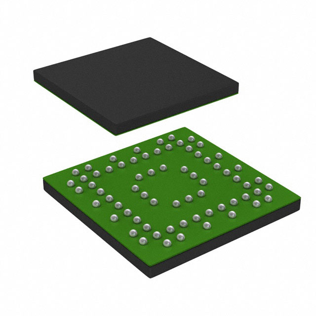
- Part No.:
- SCH3223-7U-TR
- Manufacturer:
- Microchip Technology
- Category:
- Application Specific Microcontrollers
- Package:
- 64-WFBGA
- Datasheet:
-
 SCH3223-7U-TR.pdf
- Description:
- IC CTLR IO LPC MULT PORT 64WFBGA
- Quantity:
- Payment:

- Shipping:

Inventory:4,091
Please send an inquiry. Send us your inquiry, and we will respond immediately.
Product details
Overview
SCH3223-7U-TR from Microchip Technology is a 3.3V LPC Super I/O controller with integrated hardware monitoring, dual NS16550-compatible UARTs, watchdog timer, and motherboard glue logic - supporting PC99/PC2001 and ACPI 2.0 compliance for embedded industrial motherboards requiring system-level power management, thermal supervision, and serial I/O consolidation.
For engineers reviewing the SCH3223-7U-TR datasheet, SCH3223-7U-TR pinout, SCH3223-7U-TR application, or SCH3223-7U-TR equivalent, key selection considerations include its 64-ball WFBGA package, 19 GPIOs (2 VID-capable), 3.3V core with 5V-tolerant SIO block, LPC bus operation up to 33 MHz, and hardware-monitored voltage/temperature/fan control for reliable platform management in space-constrained designs.
Technical Context
The SCH3223-7U-TR implements an LPC interface compliant with Intel Low Pin Count Specification v1.0, supporting 19–33 MHz clocking and serialized IRQ delivery to PCI systems. Its dual high-speed UARTs feature 16-byte FIFOs, programmable baud rates up to 1.5 Mbps, RS485 auto-direction control, and IRQ sharing capability.
Hardware monitoring includes four analog inputs (+2.5V, +5V, +12V, Vccp), internal/remote temperature sensing (±1.5°C accuracy), limit comparison, and one PWM-controlled fan output. Power management integrates PME wake-up via GP42/nIO_PME, SMI generation via GP27/nIO_SMI, resume reset (nRSMRST), and IDE/PCI reset buffers with software control.
Key Specifications
| Parameter | Value and Actual Design Meaning |
|---|---|
| LPC Bus Frequency | 19–33 MHz - enables direct integration into modern low-pin-count motherboard architectures without external bridge logic. |
| UART Compatibility | NS16550A - ensures drop-in replacement for legacy serial port firmware and driver stacks across BIOS and OS layers. |
| FIFO Depth | 16-byte per UART - reduces CPU interrupt load and supports sustained 1.5 Mbps data transfer without overrun errors. |
| Hardware Monitoring Inputs | +2.5V, +5V, +12V, Vccp, VCC, VTR, Vbat, remote thermal diode - provides full-system power rail and thermal visibility for autonomous fault response. |
| GPIO Count | 19 pins, including 2 VID-capable - allows flexible board-level configuration of processor voltage identification and discrete control signals. |
| Package | 64-ball WFBGA, 6 mm × 6 mm, 0.5 mm pitch - supports high-density PCB layouts while maintaining manufacturability with 0.65 mm trace routing rules. |
| Operating Temperature | −40°C to +85°C (industrial grade) - guarantees stable operation in uncontrolled environments such as factory automation and outdoor edge gateways. |
Pinout & Package
64-ball WFBGA (6 mm × 6 mm, 0.5 mm pitch), RoHS-compliant, with sparse ball array enabling 0.65 mm trace routing. Power planes separated: VCC/VSS for Super I/O logic, HVTR/HVSS for hardware monitoring block.
| Pin/Terminal | Circuit Role | Design Meaning |
|---|---|---|
| LAD[3:0] | LPC Address/Data Bus | Multiplexed command/address/data lines - carry all LPC transactions including configuration, runtime register access, and firmware updates. |
| LFRAME# | LPC Frame Signal | Indicates start/end of LPC cycle - critical for timing-critical operations like SMI assertion and PME event synchronization. |
| GP55 / nRTS2 / RESGEN | Multi-function GPIO | Configurable as RTS2 output or strap pin selecting watchdog reset pulse width (200 ms or 500 ms). |
| GP61 / nLED2 / CLKO | Programmable Output | Drives LED2 under VTR power or outputs programmable clock signal (16 Hz default) for RTC or timing reference. |
| nRSMRST | Resume Reset Output | Open-drain output asserting system resume reset - used by chipset to reinitialize memory controller and peripheral logic after S3/S4/S5 exit. |
| PWM1 | Fan Speed Control | Open-drain PWM output driving external MOSFET - enables closed-loop fan speed regulation based on monitored temperature thresholds. |
Key Features
| Feature | Design Value |
|---|---|
| Dual High-Speed UARTs | Each supports 1.5 Mbps with 16-byte FIFOs, modem control, and RS485 auto-direction - eliminates need for external UART expanders in multi-serial industrial controllers. |
| Hardware Monitoring Block | Monitors 7 voltage rails, internal/external temperature (±1.5°C), and fan tachometer - enables autonomous thermal throttling and power-rail fault detection without host CPU intervention. |
| ACPI 2.0 & PC99 Compliance | Full support for S0–S5 power states, PME wake events, and SMI generation - ensures seamless integration into standard BIOS/UEFI power management frameworks. |
| Security Key Register | 32-byte battery-backed register for device authentication - stores cryptographic keys or board-specific identifiers resistant to power-loss tampering. |
| Reset Generation Logic | Includes IDE reset output, three PCI reset buffers, and nRSMRST - replaces discrete reset logic and simplifies motherboard BOM for x86-compatible platforms. |
Applications
| Industrial Embedded Controller | Medical Diagnostic Equipment |
|---|---|
Use Scenario: Fan-cooled PLC controller operating continuously in factory ambient (−20°C to +70°C) with dual serial interfaces for Modbus RTU and barcode scanner communication. IC Role / Device Role / Timing Role: Central Super I/O managing UARTs, thermal safety shutdown, power-good sequencing, and watchdog-triggered recovery. Use Value: Eliminates discrete reset generators, voltage supervisors, and UART ICs - reducing BOM count by ≥5 components while enabling real-time thermal response within 100 ms. |
Use Scenario: Portable ultrasound imaging unit requiring battery-backed security key storage, precise +5V/+12V rail monitoring, and RS485-linked transducer calibration. IC Role / Device Role / Timing Role: Platform management hub handling power fail recovery, secure boot credential storage, and dual-serial diagnostics interface. Use Value: Battery-backed 32-byte security register preserves device identity across power cycles; remote thermal diode input enables accurate probe temperature compensation. |
| Network Appliance Gateway | Ruggedized Edge Compute Server |
Use Scenario: Fanless network gateway with two isolated serial ports for console access and out-of-band management, plus hardware-monitored PoE power supplies. IC Role / Device Role / Timing Role: LPC-connected I/O concentrator providing serial console, power sequencing, and voltage margining alerts. Use Value: 5V-tolerant SIO block interfaces directly with legacy RS232 level shifters; programmable clock output synchronizes external watchdog or RTC. |
Use Scenario: Compact server node deployed in telecom cabinets with strict thermal limits, requiring automatic fan speed adjustment and +12V supply fault logging. IC Role / Device Role / Timing Role: System health monitor generating PME wake events on overtemperature and controlling PWM fan drive via FANTACH1 feedback. Use Value: Single-chip solution replaces discrete ADC, comparator, and fan controller - cuts thermal design validation time by eliminating inter-component timing mismatches. |
Equivalent & Alternatives
The following parts are listed as comparable options for similar Super I/O controller applications.
| Alternative Part | Technical Difference | Application Difference | Selection Advice |
|---|---|---|---|
| IT8786E-S | 48-pin QFP package; lacks VID-capable GPIOs; supports only single thermal diode input. | Better suited for cost-sensitive consumer motherboards with simpler thermal requirements. | Select when footprint constraints favor QFP and VID functionality is unnecessary. |
| NCT5104D | 64-pin QFN; no LPC interface - uses ISA-style parallel configuration; lower max UART baud rate (921 kbps). | Targeted at legacy x86 designs where LPC bus is unavailable or unused. | Choose only for backward compatibility with non-LPC platforms; not suitable for new LPC-based designs. |
Compared with IT8786E-S and NCT5104D, the SCH3223-7U-TR uniquely combines industrial-grade WFBGA packaging, dual high-speed UARTs with RS485 mode, VID-capable GPIOs, and full ACPI 2.0 compliance - making it the only option among the three qualified for new rugged embedded designs requiring compact size, thermal precision, and modern power management.
Availability
SCH3223-7U-TR is available at Aetrix Electronics and suitable for industrial embedded controllers, medical diagnostic equipment, network appliance gateways, and ruggedized edge compute servers requiring stable component supply across extended product lifecycles.
Supply support for SCH3223-7U-TR includes scheduled delivery planning, volume procurement assistance, BOM continuity management, traceable sourcing, and lifecycle availability coordination for OEM customers, industrial embedded developers, connected-device designers, and electronics production programs.
Manufacturer
Microchip Technology is a global semiconductor company delivering microcontrollers, analog devices, and connectivity solutions for embedded control applications.
The SCH3223-7U-TR belongs to Microchip's Super I/O family designed specifically for x86-compatible platform management - integrating legacy I/O, hardware monitoring, and power control into a single LPC-connected device for industrial and medical motherboard designs.
FAQ
What is the maximum UART baud rate supported by the SCH3223-7U-TR?
The SCH3223-7U-TR supports UART data rates up to 1.5 Mbps per port, achieved through its NS16550A-compatible architecture and programmable baud rate generator. This capability is confirmed in DS00002028B-page 4 and enables high-throughput serial communication in industrial automation and test equipment where legacy RS232/RS485 interfaces remain essential. The SCH3223-7U-TR maintains full compatibility with standard UART drivers at these speeds.
Does the SCH3223-7U-TR support both S3 and S5 wake-up events?
Yes, the SCH3223-7U-TR supports programmable wake-up events from both S3 (suspend-to-RAM) and S5 (soft-off) states via its nIO_PME output, as documented in Section 12.0 of DS00002028B. Wake-up sources include GP42/nIO_PME, CLOCKI32, nRI1, GP50/nRI2, and other GPIOs powered by VTR - ensuring reliable system resume even when VCC is removed. This behavior is integral to the SCH3223-7U-TR's ACPI 2.0 compliance.
How many voltage rails can the SCH3223-7U-TR monitor simultaneously?
The SCH3223-7U-TR monitors seven distinct voltage rails: +2.5V, +5V, +12V, Vccp (processor core), VCC, VTR, and Vbat - as specified in DS00002028B-page 4 and Table 2-2. Each analog input is backdrive-protected and referenced to HVTR, enabling simultaneous real-time measurement without cross-rail interference. This comprehensive monitoring is a core function of the SCH3223-7U-TR's hardware monitoring block.
Is the SCH3223-7U-TR pin-compatible with earlier Microchip Super I/O devices like the SCH3112?
No, the SCH3223-7U-TR is not pin-compatible with the SCH3112. It uses a 64-ball WFBGA package versus the SCH3112's 128-pin LQFP, and its pin functions - including LPC-specific signals (LAD[3:0], LFRAME#), dedicated reset outputs (nPCIRST1–3), and hardware monitoring inputs (REMOTE1+, REMOTE1−) - differ fundamentally. Migration requires PCB redesign. This distinction is confirmed by package outlines in DS00002028B-page 188 and pin summaries in DS00002028B-page 5–6.
What is the purpose of the RESGEN function on the SCH3223-7U-TR's GP55 pin?
The RESGEN function on GP55 of the SCH3223-7U-TR selects the watchdog timer reset pulse width: an external pull-down configures 500 ms, while a pull-up sets 200 ms - as defined in DS00002028B-page 9, Note 2-11. This strapping option allows system designers to tune reset duration for specific power supply hold-up times, ensuring reliable reinitialization without premature release. The RESGEN function is exclusive to the SCH3223-7U-TR and not shared with other pins.
SCH3223-7U-TR Specifications
- Product attributes
- Attribute value
- Manufacturer:
- Microchip Technology
- Series:
- -
- Package/Case:
- 64-WFBGA
- Packaging:
- Tape & Reel (TR)
- Product Status:
- Active
- Programmable:
- Not Verified
- Applications:
- I/O Controller
- Core Processor:
- 8024 Keyboard Controller
- Program Memory Type:
- -
- Controller Series:
- -
- RAM Size:
- -
- Interface:
- LPC, Serial, UART
- Number of I/O:
- 19
- Voltage - Supply:
- -
- Operating Temperature:
- 0°C ~ 70°C (TA)
- Grade:
- -
- Qualification:
- -
- Mounting Type:
- Surface Mount
- Supplier Device Package:
- 64-WFBGA (6x6)
SCH3223-7U-TR FAQ
1.How can I place an order for SCH3223-7U-TR through Aetrix?
Please submit a Request for Quotation (RFQ) for SCH3223-7U-TR on Aetrix. Our sales agent will provide a competitive quotation and guide you through the order confirmation once you accept the terms.
2.Are the price and stock information for SCH3223-7U-TR reliable?
The price and inventory of SCH3223-7U-TR are updated periodically and may fluctuate due to market conditions. Stock and pricing data are typically refreshed every 24 hours. Quotation validity for SCH3223-7U-TR is usually 5 days.
3.What payment methods are accepted for SCH3223-7U-TR?
We accept Wire Transfer, PayPal, Credit Card, Western Union, MoneyGram, and Escrow for SCH3223-7U-TR transactions.
Note: Certain payment methods may incur a processing fee.
4.How is shipping managed for SCH3223-7U-TR?
SCH3223-7U-TR orders can be shipped via leading logistics carriers, including DHL, UPS, FedEx, TNT, or Registered Mail.
Once your SCH3223-7U-TR order is processed, you will receive an email with the shipment details and tracking number.
Note: Tracking information may take up to 24 hours to appear. Express delivery typically takes 3–5 business days.
5.How can I obtain technical support or documentation for SCH3223-7U-TR?
For technical support, including SCH3223-7U-TR datasheets, pinout diagrams, or application guidance, please contact our engineering support team. They can provide detailed documentation and assistance for your SCH3223-7U-TR requirements.
6.How does Aetrix verify that SCH3223-7U-TR is sourced from the original manufacturer or authorized distributors?
All SCH3223-7U-TR products on Aetrix are procured from qualified distributors and authorized channels. Our dedicated quality assurance team conducts strict verification, including traceability checks and, if necessary, third-party testing. This ensures that SCH3223-7U-TR meets industry standards.
7.What is the process for return or replacement of SCH3223-7U-TR?
All SCH3223-7U-TR units undergo pre-shipment inspection (PSI). If there is an issue with SCH3223-7U-TR, returns or replacements are accepted under the following conditions:
1.Quantity discrepancies, incorrect items, or visible external defects (such as breakage or corrosion), acknowledged by Aetrix.
2.The issue is reported within 90 days of delivery.
3.The SCH3223-7U-TR part is unused and in its original packaging.
Return procedure for SCH3223-7U-TR:
1.Submit a request within 90 days.
2.Obtain a Return Material Authorization (RMA) from Aetrix.
SCH3223-7U-TR Tags

-
CYPD3175-24LQXQ
Infineon Technologies

-
SLB9672VU20FW1523XTMA1
Infineon Technologies

-
SLB9670VQ20FW785XTMA1
Infineon Technologies
-
SLB9672XU20FW1523XTMA1
Infineon Technologies
-
SLB9673XU20FW2613XTMA1
Infineon Technologies

-
CYPD3125-40LQXIT
Infineon Technologies

-
AT97SC3204-U2A1A-20
Microchip Technology
-
AT97SC3204-U2A1A-10
Microchip Technology
-
SLM9670AQ20FW1311XTMA1
Infineon Technologies
-
SLB9672XU20FW1613XTMA1
Infineon Technologies
-
SLB9672AU20FW1613XTMA1
Infineon Technologies
-
SLB9673AU20FW2613XTMA1
Infineon Technologies
Tech Hub

TTL and CMOS logic families differ in thresholds, loading, output drive, power and timing. This engineering guide compares 74HC and 74HCT, calculates noise margins and checks 3.3 V/5 V compatibility.

A practical engineering guide to 3.3V and 5V logic compatibility, input thresholds, resistor dividers, translator ICs, MOSFET level shifting, I2C pull-ups, timing limits and power-sequencing risks.

The 74HC595 uses push-pull logic outputs, while the TPIC6B595 uses 50 V open-drain DMOS sinks for higher-power loads. This guide compares timing, current limits, 3.3 V interfacing, load wiring, thermal…

The 74HC595 converts serial data into eight stable parallel outputs. This guide covers pin functions, shift and storage timing, OE and MR behavior, drive-current limits, cascading, voltage compatibilit…

A technical comparison of level-sensitive latches and edge-triggered flip-flops, covering timing windows, setup and hold limits, master–slave operation, time borrowing, race-through, HDL inference and…

A D latch stores one bit while Enable controls when data can pass. This reference covers gate-level operation, truth tables, transparency, setup and hold timing, LE versus OE, common ICs and practical …

An SR latch stores one bit through cross-coupled feedback. This engineering reference covers NOR and NAND implementations, truth tables, forbidden-state recovery, gated operation, switch debouncing, fa…

Latch circuits retain one bit through feedback. This technical reference covers SR and D latches, truth tables, transparency, timing limits, latch-versus-flip-flop behavior, applications and common log…

An engineering guide to LED driver operation, constant-current and constant-voltage outputs, linear and switching topologies, dimming, IC selection, calculations, replacement compatibility, and fault c…

Operational amplifier guide covering op amp basics, feedback, ideal vs real op amps, common configurations, buffer circuits, offset, bias current, gain-bandwidth, slew rate, rail-to-rail limits and sel…


