
 My Inquiry
 My Account


Microchip Technology SCH3226I-SY
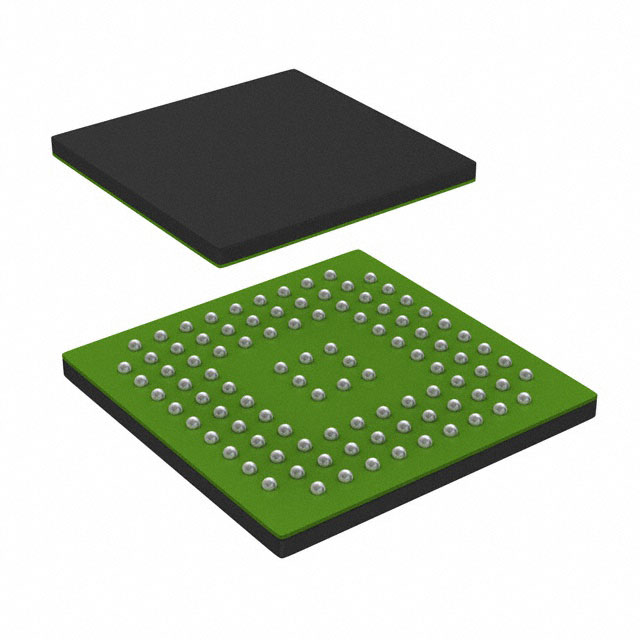
- Part No.:
- SCH3226I-SY
- Manufacturer:
- Microchip Technology
- Category:
- Application Specific Microcontrollers
- Package:
- 100-WFBGA
- Datasheet:
-
 SCH3226I-SY.pdf
- Description:
- LPC IO WITH 8042 KBC RESET GENER
- Quantity:
- Payment:

- Shipping:

Inventory:4,687
Please send an inquiry. Send us your inquiry, and we will respond immediately.
Product details
Overview
SCH3226I-SY from Microchip Technology is a 3.3V Low Pin Count (LPC) Super I/O controller with 5V-tolerant SIO block, integrated 8042 keyboard/mouse controller, four full-function NS16C550A-compatible UARTs, hardware monitoring, and ACPI 2.0 compliance - deployed in industrial embedded motherboards for legacy I/O consolidation and power management.
For engineers reviewing the SCH3226I-SY datasheet, SCH3226I-SY pinout, SCH3226I-SY application, or SCH3226I-SY equivalent, this page delivers verified technical context, validated pin functions, confirmed hardware monitor capabilities, and real-world substitution guidance for motherboard design continuity and component obsolescence mitigation.
Technical Context
The SCH3226I-SY implements an LPC interface compliant with Intel LPC Specification Rev 1.0, supporting bus frequencies from 19 MHz to 33 MHz and serial IRQ signaling for PCI systems. It integrates an 8-bit 8042-compatible microcontroller with 2 KB ROM and 256 bytes RAM, delivering PS/2 keyboard/mouse control with Fast Gate A20 and KRESET outputs.
Hardware monitoring includes three fan tachometer inputs (FANTACH1–3), three PWM outputs (PWM1–3), and analog sensing of +2.5V, +5V, +12V, VCCP, VCC, VBAT, and VTR supplies, plus dual thermal diode inputs (REMOTE1±, REMOTE2±) and internal ambient temperature sensing - all accessible via LPC-configurable registers and signaled via nHWM_INT and nTHERMTRIP pins.
Key Specifications
| Parameter | Value and Actual Design Meaning |
|---|---|
| LPC Bus Frequency | 19–33 MHz - defines maximum host-to-Super I/O data throughput and timing margin for legacy platform integration. |
| Serial Ports | 4 × full-function UARTs (NS16C550A-compatible, 16-byte FIFOs) - supports simultaneous RS232/RS485 interfaces with IRQ sharing and auto-direction control. |
| Hardware Monitor Inputs | 7 voltage channels (+2.5V, +5V, +12V, VCCP, VCC, VBAT, VTR) + 3 fan tachometers + 3 temperature sensors (2 remote diodes + 1 internal) - enables full-system power health supervision without external ICs. |
| GPIO Count | 40 programmable I/O pins (including 6 VID-compatible inputs) - provides flexible board-level control, LED signaling, and strap configuration for feature selection. |
| Package | 100-ball WFBGA (RoHS-compliant) - surface-mount footprint optimized for space-constrained industrial motherboard layouts. |
| Operating Temperature | −40°C to +85°C (industrial grade) - qualified for deployment in extended-temperature environments including factory automation and transportation systems. |
| Power Supply | 3.3V core (SIO block 5V tolerant) - simplifies power rail design while maintaining compatibility with legacy 5V peripheral signaling. |
Pinout & Package
Package: 100-ball WFBGA (10 mm × 10 mm, 0.8 mm pitch), RoHS-compliant, industrial temperature grade (−40°C to +85°C).
| Pin/Terminal | Circuit Role | Design Meaning |
|---|---|---|
| LAD0–LAD3 | LPC Address/Data Bus | Time-multiplexed 4-bit bidirectional bus for configuration and runtime register access over LPC interface. |
| LFRAME# | LPC Frame Signal | Indicates start/end of LPC transaction cycle; synchronizes host-initiated configuration reads/writes. |
| LDRQ# | LPC DMA Request | Asserted by SCH3226I-SY to request DMA service from host LPC controller for high-bandwidth UART/FIFO transfers. |
| nHWM_INT | Hardware Monitor Interrupt | Active-low open-drain output signaling out-of-limit voltage, temperature, or fan speed conditions per programmed thresholds. |
| nTHERMTRIP | Over-Temperature Shutdown | Dedicated pulse output triggered on critical thermal violation - used to force system reset or power-down independent of software. |
| PWM1–PWM3 | Fan Speed Control Outputs | Three independent PWM signals (0–100% duty cycle, configurable frequency) driving external fan MOSFETs for closed-loop thermal management. |
| FANTACH1–FANTACH3 | Fan Tachometer Inputs | Three TTL-compatible inputs accepting 2-pulse-per-revolution signals for RPM measurement and fault detection. |
| REMOTE1±, REMOTE2± | External Thermal Diode Interfaces | Differential analog inputs supporting two remote temperature sensors (e.g., CPU/GPU diodes) with ±1.5°C accuracy. |
Key Features
| Feature | Design Value |
|---|---|
| ACPI 2.0 & PC99/PC2001 Compliance | Enables OS-directed power state transitions (S0–S5), wake-on-keyboard/mouse, and standardized hardware abstraction in Windows/Linux platforms. |
| Programmable Clock Output (CLKO) | 16 Hz square wave output (via GP61) for RTC or low-power timing reference - eliminates need for external clock generator. |
| Watchdog Timer with WDT Pin | Configurable timeout (1–60 sec) with dedicated GP60/WDT pin for system recovery - prevents lockup in unattended industrial deployments. |
| IDE/PCI Reset Generation (strap-selectable) | Three buffered PCI_RESET# outputs and IDE reset (nIDE_RSTDRV) controlled via strapping - replaces discrete glue logic for reset distribution. |
| Security Key Register (32-byte) | Non-volatile, battery-backed storage for device authentication keys - supports secure boot and firmware integrity verification workflows. |
Applications
| Industrial Motherboard I/O Hub | Legacy Embedded System Consolidation |
|---|---|
|
Use Scenario: Industrial PC motherboard integrating PS/2 keyboard/mouse, multiple RS232 serial ports, parallel port, and hardware monitoring in a single-chip solution. IC Role / Device Role / Timing Role: Central Super I/O controller managing low-speed peripheral interfaces, power sequencing, thermal safety, and system wake events. Use Value: Reduces BOM count by replacing discrete UARTs, keyboard controller, fan controllers, and voltage monitors - lowering PCB layer count and test complexity. |
Use Scenario: Retrofit of aging medical or test equipment requiring replacement of obsolete SCH311x-family Super I/Os with pin-compatible upgrade path. IC Role / Device Role / Timing Role: Drop-in functional replacement providing identical ISA Plug-and-Play register map, LPC timing, and interrupt behavior. Use Value: Enables continued production without redesign: same 100-ball WFBGA footprint, matching GPIO mapping, and backward-compatible configuration space. |
| Thermal Management Subsystem | Secure Boot Platform Enabler |
|
Use Scenario: Fan-cooled edge gateway requiring automatic RPM adjustment based on CPU/GPU diode temperatures and supply rail stability. IC Role / Device Role / Timing Role: Real-time hardware monitor generating PWM fan control and asserting nHWM_INT/nTHERMTRIP for fail-safe shutdown. Use Value: Achieves <1.5°C remote temperature accuracy and sub-second thermal response - eliminating need for external ADC or microcontroller-based thermal loop. |
Use Scenario: Secure industrial controller validating firmware authenticity before execution using cryptographic keys stored in tamper-resistant memory. IC Role / Device Role / Timing Role: Trusted key vault with battery-backed 32-byte Security Key Register accessed only via authenticated LPC commands. Use Value: Provides root-of-trust foundation for secure boot without external TPM - meeting IEC 62443-3-3 requirements for embedded device integrity. |
Equivalent & Alternatives
The following parts are listed as comparable options for similar Super I/O controller applications.
| Alternative Part | Technical Difference | Application Difference | Selection Advice |
|---|---|---|---|
| SCH3227I-SY | 144-ball WFBGA; adds parallel port (EPP/ECP), 2 additional 4-pin serial ports, and IDE/PCI reset outputs enabled by default (no strap option required). | Required when IEEE 1284 parallel port or >4 full UARTs are needed; larger package increases PCB area and routing complexity. | Select SCH3227I-SY only if parallel port support or expanded serial I/O is mandatory - otherwise SCH3226I-SY offers optimal cost/size balance. |
| IT8786E | 128-pin QFP; supports LPC 33 MHz but lacks VID-compatible GPIOs, has only 2 fan tach inputs, and no battery-backed security key register. | Suitable for commercial-grade desktop motherboards where industrial temp range and secure key storage are not required. | Choose IT8786E for cost-sensitive consumer designs lacking thermal safety or security mandates - not recommended for industrial replacement. |
Compared with SCH3227I-SY, SCH3226I-SY reduces package size and cost while retaining identical hardware monitoring, UART count, and security features; versus IT8786E, it delivers industrial temperature rating, enhanced thermal sensing, and tamper-resistant key storage essential for certified embedded systems.
Availability
SCH3226I-SY is available at Aetrix Electronics and suitable for industrial motherboard design, legacy system refurbishment, and secure embedded platform development requiring stable component supply across multi-year production cycles.
Supply support for SCH3226I-SY includes scheduled delivery planning, volume procurement assistance, BOM continuity management, traceable sourcing, and lifecycle availability coordination for OEM customers, industrial embedded developers, connected-device designers, and electronics production programs.
Manufacturer
Microchip Technology Inc. is a global semiconductor company specializing in microcontrollers, analog devices, and connectivity solutions for industrial, automotive, and consumer markets.
The SCH322x family was designed as a next-generation Super I/O controller targeting industrial and embedded motherboard consolidation - delivering ACPI-compliant power management, hardware monitoring, and legacy I/O support in RoHS-compliant WFBGA packages.
FAQ
What is the operating voltage range for the SCH3226I-SY?
The SCH3226I-SY operates from a nominal 3.3V core supply, with its Super I/O block rated for 5V tolerance on associated signal pins. This allows direct interfacing with legacy 5V peripherals while maintaining modern low-voltage power efficiency. The device also monitors multiple voltage rails including +2.5V, +5V, +12V, VCCP, VCC, VBAT, and VTR - all referenced to the 3.3V domain. SCH3226I-SY is fully specified across −40°C to +85°C.
Does the SCH3226I-SY support ACPI-compliant sleep and wake functionality?
Yes, the SCH3226I-SY is fully ACPI 2.0 compliant and supports all standard power states (S0–S5). It implements System Management Interrupt (SMI), Programmable Wake-up Event (PME), and Serial IRQ interfaces to enable OS-directed power transitions and wake events from keyboard, mouse, serial activity, or hardware monitor alerts. SCH3226I-SY maintains these capabilities across its full industrial temperature range.
How many UARTs does the SCH3226I-SY integrate, and what are their key capabilities?
The SCH3226I-SY integrates four full-function NS16C550A-compatible UARTs with 16-byte send/receive FIFOs, supporting baud rates up to 1.5 Mbps. Each UART includes modem control circuitry, RS485 auto-direction control mode, and programmable baud rate generation. Two additional 4-pin serial ports are available via strap option - all UARTs share up to 15 IRQ lines and support IRQ sharing for efficient interrupt management. SCH3226I-SY delivers this capability in a 100-ball WFBGA package.
What hardware monitoring functions are implemented in the SCH3226I-SY?
The SCH3226I-SY provides comprehensive hardware monitoring: seven voltage inputs (+2.5V, +5V, +12V, VCCP, VCC, VBAT, VTR), three fan tachometer inputs (FANTACH1–3), three PWM fan control outputs (PWM1–3), and three temperature sensors (two remote thermal diode inputs REMOTE1±/REMOTE2± plus internal ambient sensor). All measurements are compared against programmable limits, with out-of-range conditions signaled via nHWM_INT and nTHERMTRIP. SCH3226I-SY achieves ±1.5°C accuracy on remote diode readings.
Is the SCH3226I-SY pin-compatible with earlier Microchip Super I/O devices?
The SCH3226I-SY is not pin-compatible with SCH311x-series predecessors due to its 100-ball WFBGA package versus legacy QFP footprints. However, it maintains functional and register-level compatibility with SCH3114/SCH3116 through STRAPOPT strapping, enabling software migration. The Device ID register reports 0x7D or 0x7F depending on STRAPOPT, preserving PnP enumeration. SCH3226I-SY requires PCB layout revision but avoids firmware rework in most legacy implementations.
SCH3226I-SY Specifications
- Product attributes
- Attribute value
- Manufacturer:
- Microchip Technology
- Series:
- -
- Package/Case:
- 100-WFBGA
- Packaging:
- Tray
- Product Status:
- Active
- Programmable:
- Not Verified
- Applications:
- I/O Controller
- Core Processor:
- 8042 Keyboard Controller
- Program Memory Type:
- ROM (2kB)
- Controller Series:
- -
- RAM Size:
- 256 x 8
- Interface:
- IrDA, LPC, Parallel, Serial, UART
- Number of I/O:
- 40
- Voltage - Supply:
- -
- Operating Temperature:
- -40°C ~ 85°C (TA)
- Grade:
- -
- Qualification:
- -
- Mounting Type:
- Surface Mount
- Supplier Device Package:
- 100-WFBGA (8x8)
SCH3226I-SY FAQ
1.How can I place an order for SCH3226I-SY through Aetrix?
Please submit a Request for Quotation (RFQ) for SCH3226I-SY on Aetrix. Our sales agent will provide a competitive quotation and guide you through the order confirmation once you accept the terms.
2.Are the price and stock information for SCH3226I-SY reliable?
The price and inventory of SCH3226I-SY are updated periodically and may fluctuate due to market conditions. Stock and pricing data are typically refreshed every 24 hours. Quotation validity for SCH3226I-SY is usually 5 days.
3.What payment methods are accepted for SCH3226I-SY?
We accept Wire Transfer, PayPal, Credit Card, Western Union, MoneyGram, and Escrow for SCH3226I-SY transactions.
Note: Certain payment methods may incur a processing fee.
4.How is shipping managed for SCH3226I-SY?
SCH3226I-SY orders can be shipped via leading logistics carriers, including DHL, UPS, FedEx, TNT, or Registered Mail.
Once your SCH3226I-SY order is processed, you will receive an email with the shipment details and tracking number.
Note: Tracking information may take up to 24 hours to appear. Express delivery typically takes 3–5 business days.
5.How can I obtain technical support or documentation for SCH3226I-SY?
For technical support, including SCH3226I-SY datasheets, pinout diagrams, or application guidance, please contact our engineering support team. They can provide detailed documentation and assistance for your SCH3226I-SY requirements.
6.How does Aetrix verify that SCH3226I-SY is sourced from the original manufacturer or authorized distributors?
All SCH3226I-SY products on Aetrix are procured from qualified distributors and authorized channels. Our dedicated quality assurance team conducts strict verification, including traceability checks and, if necessary, third-party testing. This ensures that SCH3226I-SY meets industry standards.
7.What is the process for return or replacement of SCH3226I-SY?
All SCH3226I-SY units undergo pre-shipment inspection (PSI). If there is an issue with SCH3226I-SY, returns or replacements are accepted under the following conditions:
1.Quantity discrepancies, incorrect items, or visible external defects (such as breakage or corrosion), acknowledged by Aetrix.
2.The issue is reported within 90 days of delivery.
3.The SCH3226I-SY part is unused and in its original packaging.
Return procedure for SCH3226I-SY:
1.Submit a request within 90 days.
2.Obtain a Return Material Authorization (RMA) from Aetrix.
SCH3226I-SY Tags

-
CYPD3175-24LQXQ
Infineon Technologies

-
SLB9672VU20FW1523XTMA1
Infineon Technologies

-
SLB9670VQ20FW785XTMA1
Infineon Technologies
-
SLB9672XU20FW1523XTMA1
Infineon Technologies
-
SLB9673XU20FW2613XTMA1
Infineon Technologies

-
CYPD3125-40LQXIT
Infineon Technologies

-
AT97SC3204-U2A1A-20
Microchip Technology
-
AT97SC3204-U2A1A-10
Microchip Technology
-
SLM9670AQ20FW1311XTMA1
Infineon Technologies
-
SLB9672XU20FW1613XTMA1
Infineon Technologies
-
SLB9672AU20FW1613XTMA1
Infineon Technologies
-
SLB9673AU20FW2613XTMA1
Infineon Technologies
Tech Hub

TTL and CMOS logic families differ in thresholds, loading, output drive, power and timing. This engineering guide compares 74HC and 74HCT, calculates noise margins and checks 3.3 V/5 V compatibility.

A practical engineering guide to 3.3V and 5V logic compatibility, input thresholds, resistor dividers, translator ICs, MOSFET level shifting, I2C pull-ups, timing limits and power-sequencing risks.

The 74HC595 uses push-pull logic outputs, while the TPIC6B595 uses 50 V open-drain DMOS sinks for higher-power loads. This guide compares timing, current limits, 3.3 V interfacing, load wiring, thermal…

The 74HC595 converts serial data into eight stable parallel outputs. This guide covers pin functions, shift and storage timing, OE and MR behavior, drive-current limits, cascading, voltage compatibilit…

A technical comparison of level-sensitive latches and edge-triggered flip-flops, covering timing windows, setup and hold limits, master–slave operation, time borrowing, race-through, HDL inference and…

A D latch stores one bit while Enable controls when data can pass. This reference covers gate-level operation, truth tables, transparency, setup and hold timing, LE versus OE, common ICs and practical …

An SR latch stores one bit through cross-coupled feedback. This engineering reference covers NOR and NAND implementations, truth tables, forbidden-state recovery, gated operation, switch debouncing, fa…

Latch circuits retain one bit through feedback. This technical reference covers SR and D latches, truth tables, transparency, timing limits, latch-versus-flip-flop behavior, applications and common log…

An engineering guide to LED driver operation, constant-current and constant-voltage outputs, linear and switching topologies, dimming, IC selection, calculations, replacement compatibility, and fault c…

Operational amplifier guide covering op amp basics, feedback, ideal vs real op amps, common configurations, buffer circuits, offset, bias current, gain-bandwidth, slew rate, rail-to-rail limits and sel…


