
 My Inquiry
 My Account


STMicroelectronics STA515W13TR
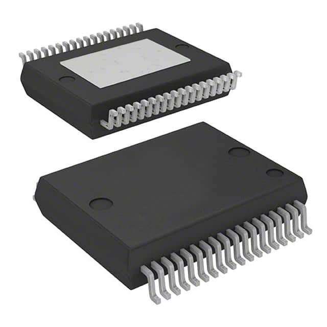
- Part No.:
- STA515W13TR
- Manufacturer:
- STMicroelectronics
- Category:
- Audio Amplifiers
- Package:
- 36-PowerBFSOP (0.295", 7.50mm Width)
- Datasheet:
-
 STA515W13TR.pdf
- Description:
- IC AMP D QUAD 10W POWERSSO36
- Quantity:
- Payment:

- Shipping:

Inventory:1,663
Please send an inquiry. Send us your inquiry, and we will respond immediately.
Product details
Overview
STA515W13TR from STMicroelectronics is a monolithic quad half-bridge power stage in Multipower BCD technology, designed as the output stage for stereo all-digital high-efficiency amplifiers. It delivers 10 W × 4 channels into 4 Ω (10% THD, VCC = 18 V, single-ended), or 20 W + 20 W into 8 Ω (BTL), or 40 W into 8 Ω (parallel-BTL, VCC = 26 V). Key confirmed parameters: 40 V max supply, 3 A continuous output current, 200 mΩ RdsON, thermal warning at 130 °C, and undervoltage lockout at 7 V.
For engineers reviewing the STA515W13TR datasheet, STA515W13TR pinout, STA515W13TR application, or STA515W13TR equivalent, this page provides verified electrical specifications, PowerSSO36 EPD package mapping, dual/quad bridge configuration logic, thermal protection behavior, and real-world audio amplifier use cases with DDX and binary PWM modes.
Technical Context
The STA515W13TR implements four independent half-bridge stages with complementary DMOS outputs, configurable via CONFIG pin to operate as two full H-bridges or one high-current parallel bridge. Its logic interface accepts CMOS-compatible inputs referenced to VL (2.7–5.0 V), with input thresholds scaling proportionally to VL voltage.
Protection architecture includes open-drain FAULT (short-circuit/thermal fault) and THWARN (130 °C thermal warning) outputs, undervoltage lockout (7 V), and automatic recovery mode when FAULT and TRISTATE pins are tied through an RC network. Dead time is dynamically adjusted: ≤50 ns under high-current switching (L = 22 μH, C = 470 nF, IDD = 3.0 A).
Key Specifications
| Parameter | Value and Actual Design Meaning |
|---|---|
| VCC Max | 40 V - Absolute maximum DC supply voltage across all power pins (4, 7, 12, 15) |
| RdsON | 200 mΩ typ - On-resistance per MOSFET channel enables low conduction loss at 3 A load current |
| Output Config | Quad half-bridge - Supports dual full-bridge (20 W × 2 @ 8 Ω) or parallel-BTL (40 W @ 8 Ω) via CONFIG pin |
| Thermal Warning | 130 °C - Open-drain THWARN asserts low before thermal shutdown (150 °C), enabling preemptive system response |
| Undervoltage Lockout | 7 V - Disables outputs until VCC rises above threshold, preventing erratic operation during brownout |
| Logic Compatibility | CMOS - Inputs accept 2.7–5.0 V logic levels; thresholds scale with VL pin voltage (e.g., VIN-HIGH = VL/2 + 300 mV) |
| Package Thermal RθJC | 1.5 °C/W - Junction-to-case resistance measured at thermal pad, critical for heatsink design in 21 W Ptot operation |
Pinout & Package
The STA515W13TR is housed in a 36-pin PowerSSO package with exposed pad down (EPD), optimized for thermal dissipation in audio power applications. The exposed thermal pad must be soldered to PCB copper for effective heat transfer.
| Pin/Terminal | Circuit Role | Design Meaning |
|---|---|---|
| 1 GNDSUB | Substrate ground | Internal die substrate connection; must be tied to main system ground plane |
| 2,3 OUT2B | Half-bridge 2B output | Low-side output node of second half-bridge; connects to speaker negative terminal in BTL mode |
| 4 VCC2B | Positive supply for OUT2B | Power rail for N-channel MOSFET in half-bridge 2B; requires local 100 nF decoupling |
| 5,6 GND2B/GND2A | Negative supply return | Dedicated ground paths for second half-bridge; must be short-traced to minimize EMI and shoot-through risk |
| 10,11 OUT1B | Half-bridge 1B output | Low-side output of first half-bridge; used with OUT1A to form full H-bridge driving left channel |
| 24 CONFIG | Configuration control | Logic-high (to VDD) enables parallel-output mode for doubled current capability; logic-low enables standard dual-bridge operation |
| 27 FAULT | Fault indicator | Open-drain output pulled low during overcurrent or thermal fault; requires external 10 kΩ pull-up to VDD |
| 29–32 IN1A/IN1B/IN2A/IN2B | Bridge control inputs | CMOS-level timing signals defining H-bridge state (positive/negative/dump/Hi-Z); referenced to VL voltage |
Key Features
| Feature | Design Value |
|---|---|
| Multipower BCD process | Enables monolithic integration of high-voltage DMOS power transistors, bipolar drivers, and CMOS logic on single die |
| Configurable topology | Single pin (CONFIG) selects between dual full-bridge or parallel-BTL operation-no external hardware change required |
| Dynamic dead-time control | Adjusts turn-off/turn-on delays (<50 ns max) based on load current to prevent cross-conduction while minimizing distortion |
| Thermal warning with hysteresis | THWARN activates at 130 °C and releases at 105 °C (25 °C hysteresis), enabling graceful power reduction before shutdown |
| Auto-recovery fault handling | When FAULT and TRISTATE are shorted via RC network, device self-resets after fault clears-eliminates need for MCU intervention |
Applications
| Home Audio Amplifier | Automotive Infotainment Output Stage |
|---|---|
|
Use Scenario: 4-channel stereo amplifier delivering 10 W per channel into 4 Ω speakers in compact AV receivers. IC Role / Device Role / Timing Role: Quad half-bridge output stage converting DDX-modulated PWM signals into analog audio power; driven by STA308 digital audio processor. Use Value: Enables Class-D efficiency (>90%) with low RdsON and integrated protection, reducing heatsink size and eliminating discrete driver ICs. |
Use Scenario: Dual full-bridge configuration powering front left/right speakers (20 W × 2 @ 8 Ω) in vehicle head units. IC Role / Device Role / Timing Role: High-current H-bridge driver accepting binary PWM inputs; CONFIG pin held low for standard dual-bridge operation. Use Value: Withstand automotive load dump (40 V transient) and ambient temps up to 70 °C; undervoltage lockout prevents pop-noise during ignition cycling. |
| Active Subwoofer Power Module | Professional Audio Reference Design |
|
Use Scenario: Single parallel-BTL mode (CONFIG = VDD) delivering 40 W into 8 Ω subwoofer driver using STA515W13TR + STA308. IC Role / Device Role / Timing Role: Current-doubled output stage where OUT1A/OUT1B and OUT2A/OUT2B are paralleled per channel under synchronized DDX control. Use Value: Doubles output current capability without external current-sharing components; thermal warning allows DSP-based power limiting before shutdown. |
Use Scenario: Evaluation platform for DDX modulation schemes using ST's STA308+STA515W13TR reference board (e.g., STEVAL-ILL001V1). IC Role / Device Role / Timing Role: Pin-compatible drop-in replacement for legacy quad half-bridges; TRISTATE and FAULT pins enable automated test sequencing. Use Value: Simplified validation of thermal management, EMI filtering, and protection response-verified against ST's documented 22 μH/470 nF filter design. |
Equivalent & Alternatives
The following parts are listed as comparable options for similar quad half-bridge amplifier applications.
| Alternative Part | Technical Difference | Application Difference | Selection Advice |
|---|---|---|---|
| TAS5381AIPAG | 36-V max, 4.5-A peak, 120 mΩ RdsON, integrated gate drivers, no CONFIG pin for parallel mode | Designed for TI PurePath™ digital input; lacks thermal warning pin and auto-recovery fault mode | Choose for higher peak current and tighter RdsON tolerance, but requires external thermal monitoring and MCU-controlled fault reset |
| IRS2092SPBF | 600-V high-side/lower-side driver pair (not integrated power stage); requires external MOSFETs and bootstrap circuitry | Targeted at discrete Class-D designs with custom power FET selection; no built-in protection or regulation | Choose when discrete FET optimization (e.g., SiC, GaN) or >40 V operation is required; adds layout complexity and component count |
Compared with TAS5381AIPAG and IRS2092SPBF, the STA515W13TR uniquely integrates thermal warning, CONFIG-driven topology reconfiguration, and auto-recovery fault handling-reducing system-level BOM count and firmware overhead in cost-sensitive consumer audio designs.
Availability
STA515W13TR is available at Aetrix Electronics and suitable for home audio amplifiers, automotive infotainment systems, and active subwoofer modules requiring stable component supply across industrial temperature range (0 to 70 °C) and long-lifecycle support.
Supply support for STA515W13TR includes scheduled delivery planning, volume procurement assistance, BOM continuity management, traceable sourcing, and lifecycle availability coordination for OEM customers, industrial embedded developers, connected-device designers, and electronics production programs.
Manufacturer
STMicroelectronics is a global semiconductor leader headquartered in Geneva, Switzerland, designing and manufacturing microcontrollers, power ICs, sensors, and analog devices for industrial, automotive, and consumer markets.
The STA515W13TR belongs to ST's STA5xx family of digital audio power amplifiers, engineered specifically for high-efficiency, low-EMI Class-D audio output stages in space-constrained consumer and professional audio equipment.
FAQ
What is the function of the CONFIG pin, and how does it affect output configuration?
The CONFIG pin selects between dual full-bridge and parallel-BTL operation: logic-low (0 V) configures two independent H-bridges (20 W × 2 @ 8 Ω); logic-high (tied to VDD) enables parallel connection of OUT1A/OUT2A and OUT1B/OUT2B for 40 W into 8 Ω. This reconfiguration requires synchronized IN1A/IN2A and IN1B/IN2B inputs and matching output LC filters.
How does the thermal warning (THWARN) differ from thermal shutdown, and what design actions does it enable?
THWARN asserts low at 130 °C-20 °C before thermal shutdown (150 °C)-providing early warning to reduce PWM duty cycle or mute audio. Its open-drain output requires a 10 kΩ pull-up to VDD. Unlike FAULT, THWARN does not disable outputs; it enables proactive thermal management in DSP-controlled systems without interrupting playback.
Can the STA515W13TR drive 4 Ω loads in BTL mode, and what are the voltage and current limits?
Yes: in BTL configuration, it delivers 20 W + 20 W into 8 Ω at VCC = 18 V (10% THD), and up to 40 W into 4 Ω at VCC = 19 V (per Figure 8). Absolute maximum VCC is 40 V, and continuous output current is rated at 3 A per half-bridge; peak current capability exceeds 4.5 A under short-duration conditions with proper thermal design.
What are the critical PCB layout requirements for the PowerSSO36 EPD package?
The exposed thermal pad (EPD) must be fully soldered to a large internal or bottom-layer copper pour connected to GNDSUB (Pin 1) with ≥6 thermal vias (0.3 mm diameter, 0.6 mm pitch). Power traces (VCCx, OUTx) require ≥0.5 mm width and separate ground returns; INx and VL traces must be routed away from noisy power paths to avoid logic threshold instability.
STA515W13TR Specifications
- Product attributes
- Attribute value
- Manufacturer:
- STMicroelectronics
- Series:
- -
- Package/Case:
- 36-PowerBFSOP (0.295", 7.50mm Width)
- Packaging:
- Tape & Reel (TR)
- Product Status:
- Active
- Type:
- Class D
- Output Type:
- 4-Channel (Quad)
- Max Output Power x Channels @ Load:
- 10W x 4 @ 4Ohm
- Voltage - Supply:
- 10V ~ 36V
- Features:
- Short-Circuit and Thermal Protection
- Mounting Type:
- Surface Mount
- Operating Temperature:
- 0°C ~ 70°C (TA)
- Grade:
- -
- Qualification:
- -
- Supplier Device Package:
- PowerSSO-36 EPD
STA515W13TR FAQ
1.How can I place an order for STA515W13TR through Aetrix?
Please submit a Request for Quotation (RFQ) for STA515W13TR on Aetrix. Our sales agent will provide a competitive quotation and guide you through the order confirmation once you accept the terms.
2.Are the price and stock information for STA515W13TR reliable?
The price and inventory of STA515W13TR are updated periodically and may fluctuate due to market conditions. Stock and pricing data are typically refreshed every 24 hours. Quotation validity for STA515W13TR is usually 5 days.
3.What payment methods are accepted for STA515W13TR?
We accept Wire Transfer, PayPal, Credit Card, Western Union, MoneyGram, and Escrow for STA515W13TR transactions.
Note: Certain payment methods may incur a processing fee.
4.How is shipping managed for STA515W13TR?
STA515W13TR orders can be shipped via leading logistics carriers, including DHL, UPS, FedEx, TNT, or Registered Mail.
Once your STA515W13TR order is processed, you will receive an email with the shipment details and tracking number.
Note: Tracking information may take up to 24 hours to appear. Express delivery typically takes 3–5 business days.
5.How can I obtain technical support or documentation for STA515W13TR?
For technical support, including STA515W13TR datasheets, pinout diagrams, or application guidance, please contact our engineering support team. They can provide detailed documentation and assistance for your STA515W13TR requirements.
6.How does Aetrix verify that STA515W13TR is sourced from the original manufacturer or authorized distributors?
All STA515W13TR products on Aetrix are procured from qualified distributors and authorized channels. Our dedicated quality assurance team conducts strict verification, including traceability checks and, if necessary, third-party testing. This ensures that STA515W13TR meets industry standards.
7.What is the process for return or replacement of STA515W13TR?
All STA515W13TR units undergo pre-shipment inspection (PSI). If there is an issue with STA515W13TR, returns or replacements are accepted under the following conditions:
1.Quantity discrepancies, incorrect items, or visible external defects (such as breakage or corrosion), acknowledged by Aetrix.
2.The issue is reported within 90 days of delivery.
3.The STA515W13TR part is unused and in its original packaging.
Return procedure for STA515W13TR:
1.Submit a request within 90 days.
2.Obtain a Return Material Authorization (RMA) from Aetrix.
STA515W13TR Tags
-Exposed-Pad.jpg)
-
TS34119CS RLG
Taiwan Semiconductor Corporation

-
LM386MX-1/NOPB
Texas Instruments

-
TPA711DGNR
Texas Instruments

-
LM386N-4/NOPB
Texas Instruments

-
TS4990IST
STMicroelectronics
-
PAM8302AASCR
Diodes Incorporated
-
TPA6130A2RTJR
Texas Instruments
-
TPA6111A2DGNR
Texas Instruments
-
LM4861MX/NOPB
Texas Instruments
-
LM386M-1/NOPB
Texas Instruments

-
NCS2211DR2G
onsemi
-
IS31AP2005-DLS2-TR
Lumissil Microsystems
Tech Hub

A practical engineering and sourcing framework covering lifecycle verification, lifetime-buy calculations, replacement qualification, supplier checks and counterfeit-risk controls.

TTL and CMOS logic families differ in thresholds, loading, output drive, power and timing. This engineering guide compares 74HC and 74HCT, calculates noise margins and checks 3.3 V/5 V compatibility.

A practical engineering guide to 3.3V and 5V logic compatibility, input thresholds, resistor dividers, translator ICs, MOSFET level shifting, I2C pull-ups, timing limits and power-sequencing risks.

The 74HC595 uses push-pull logic outputs, while the TPIC6B595 uses 50 V open-drain DMOS sinks for higher-power loads. This guide compares timing, current limits, 3.3 V interfacing, load wiring, thermal…

The 74HC595 converts serial data into eight stable parallel outputs. This guide covers pin functions, shift and storage timing, OE and MR behavior, drive-current limits, cascading, voltage compatibilit…

A technical comparison of level-sensitive latches and edge-triggered flip-flops, covering timing windows, setup and hold limits, master–slave operation, time borrowing, race-through, HDL inference and…

A D latch stores one bit while Enable controls when data can pass. This reference covers gate-level operation, truth tables, transparency, setup and hold timing, LE versus OE, common ICs and practical …

An SR latch stores one bit through cross-coupled feedback. This engineering reference covers NOR and NAND implementations, truth tables, forbidden-state recovery, gated operation, switch debouncing, fa…

Latch circuits retain one bit through feedback. This technical reference covers SR and D latches, truth tables, transparency, timing limits, latch-versus-flip-flop behavior, applications and common log…

An engineering guide to LED driver operation, constant-current and constant-voltage outputs, linear and switching topologies, dimming, IC selection, calculations, replacement compatibility, and fault c…


