
 My Inquiry
 My Account


STMicroelectronics STBP110CVDJ6F
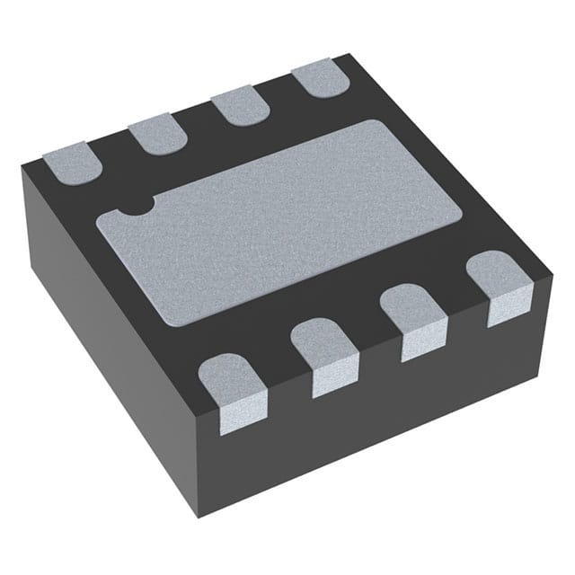
- Part No.:
- STBP110CVDJ6F
- Manufacturer:
- STMicroelectronics
- Category:
- Surge Suppression Ics
- Package:
- 8-WFDFN Exposed Pad
- Datasheet:
-
 STBP110CVDJ6F.pdf
- Description:
- IC OVP PROTECTION POWERFLAT2X2
- Quantity:
- Payment:

- Shipping:

Inventory:6,813
Please send an inquiry. Send us your inquiry, and we will respond immediately.
Product details
Overview
STBP110CVDJ6F from STMicroelectronics is an overvoltage protection device featuring an integrated 170 mΩ N-channel MOSFET switch, 28 V input overvoltage lockout (OVLO), 1.2 A continuous current rating, thermal shutdown with 20 °C hysteresis, and soft-start control for inrush current limiting. It operates in portable power rails of smartphones and digital cameras to safeguard downstream ICs from DC supply faults.
For engineers reviewing the STBP110CVDJ6F datasheet, STBP110CVDJ6F pinout, STBP110CVDJ6F application, or STBP110CVDJ6F equivalent, key selection criteria include OVLO threshold accuracy (28 V ±5%), FLT open-drain fault signaling timing (trec = 12 ms typ.), EN active-low enable logic with internal 250 kΩ pull-down, and TDFN-8 thermal pad layout requirements for junction temperature control under 1.2 A load.
Technical Context
The STBP110CVDJ6F implements a single-chip overvoltage protection solution using an internal high-voltage N-channel MOSFET controlled by analog comparators monitoring VIN against UVLO (typically 3.8 V) and OVLO (28 V) thresholds with built-in hysteresis. Its charge pump enables full gate drive for low RDS(on) operation without external bias.
Operation includes three fault responses: immediate MOSFET turn-off on OVLO detection, thermal shutdown at TJ ≥ 145 °C (with 20 °C hysteresis), and UVLO-based disable below 3.8 V. The FLT output asserts low during any active fault condition and enters high-impedance state when EN is high or VIN < UVLO.
Key Specifications
| Parameter | Value and Actual Design Meaning |
|---|---|
| OVLO Threshold | 28 V ±5% - disconnects output before damage to 5 V/3.3 V system rails |
| RDS(on) | 170 mΩ max at 25 °C - limits conduction loss to ≤205 mW at 1.2 A |
| Continuous Current | 1.2 A - supports USB-powered peripherals and battery charging circuits |
| Soft-Start Time (ton) | 1.5 ms typ. - controls inrush into 10–100 µF output capacitors |
| FLT Response Delay (toff) | 1.2 µs typ. - enables fast fault reporting to host MCU interrupt |
| Thermal Shutdown | 145 °C with 20 °C hysteresis - prevents permanent silicon damage during sustained overload |
| ESD Protection | ±15 kV air, ±8 kV contact (with 1 µF IN capacitor) - meets IEC 61000-4-2 Level 4 |
Pinout & Package
STBP110CVDJ6F uses a RoHS-compliant 2 mm × 2 mm × 0.75 mm TDFN-8 package with exposed thermal pad connected internally to GND. The pad must be soldered to a PCB thermal plane for effective junction temperature management under 1.2 A load.
| Pin/Terminal | Circuit Role | Design Meaning |
|---|---|---|
| 1 IN | Input supply rail | Accepts up to +28 V DC; requires ≥1 µF ceramic decoupling capacitor placed adjacent to pin |
| 2 GND | Power ground reference | Reference for all voltages; connects internally to exposed thermal pad |
| 3, 6, 7 NC | No-connect terminals | May be left floating or tied to GND; no internal connection |
| 4 FLT | Fault indication output | Active-low open-drain signal; pulled low during OVLO or thermal shutdown; Hi-Z when disabled or under UVLO |
| 5 EN | Enable control input | Active-low logic; internal 250 kΩ pull-down; drives MOSFET off when high |
| 8 OUT | Protected output rail | Delivers regulated input voltage to downstream circuitry when enabled and within safe operating area |
Key Features
| Feature | Design Value |
|---|---|
| Integrated charge pump | Enables full enhancement of internal N-MOSFET without external gate bias supply |
| Reverse current capability | MOSFET body diode allows OUT-to-IN current flow for peripheral powering; optional Schottky blocking diode supported |
| YD/T 1591-2006 compliance | Validated overvoltage protection performance per China Communications Standard for mobile device adapters |
| Soft-start control | Programmable 1.5 ms startup delay limits peak inrush into large output capacitance loads |
| Robust ESD protection | ±15 kV air discharge rating ensures survivability in handheld device assembly and end-user handling |
Applications
| Smartphone Power Input Protection | Digital Camera DC Adapter Interface |
|---|---|
|
Use Scenario: USB-C or barrel-jack adapter input subjected to transient overvoltage events during hot-plug or faulty charger use. IC Role / Device Role / Timing Role: Primary overvoltage guard between adapter and PMIC/battery charger; responds within 1.2 µs to disconnect rail. Use Value: Prevents catastrophic failure of 3.3 V/1.8 V application processors and memory by enforcing hard 28 V clamp before downstream LDOs saturate. |
Use Scenario: External 9 V adapter powering image sensor, ISP, and flash LED driver in compact camera module. IC Role / Device Role / Timing Role: Input rail supervisor with thermal-aware shutdown; monitors both voltage and junction temperature during burst-mode flash charging. Use Value: Maintains system uptime by allowing recovery after transient overvoltage (trec = 12 ms) while blocking sustained overtemperature via irreversible thermal latch-off. |
| PDA System-Level Power Sequencing | MP3 Player Battery Charging Path |
|
Use Scenario: Multi-rail PDA requiring coordinated power-up of core, I/O, and display supplies from shared DC input. IC Role / Device Role / Timing Role: First-stage protector enabling sequenced enablement of downstream DC-DC converters via EN pin control and FLT status feedback. Use Value: Enables deterministic boot sequence by asserting FLT to halt PMIC enable until input stabilizes above UVLO (3.8 V) and remains below OVLO (28 V). |
Use Scenario: Portable audio player accepting 5 V USB power while charging Li-ion battery through linear or switching charger IC. IC Role / Device Role / Timing Role: Fault-isolating switch between USB port and charger input; blocks reverse current leakage when battery voltage exceeds USB rail. Use Value: Eliminates need for external blocking diode by leveraging MOSFET bidirectional conduction-reducing forward drop from 0.3 V (Schottky) to 205 mV at 1.2 A. |
Equivalent & Alternatives
The following parts are listed as comparable options for similar overvoltage protection applications.
| Alternative Part | Technical Difference | Application Difference | Selection Advice |
|---|---|---|---|
| TUSB544RGER | USB 3.1 re-driver with integrated 5.5 V OVLO; no thermal shutdown or FLT output | Designed for high-speed signal integrity, not power rail protection | Select only if signal conditioning is primary requirement and OVLO is secondary |
| TPS259210DRCR | 2.7–18 V input range; 14 V fixed OVLO; higher RDS(on) (85 mΩ @ 5 V gate drive) | Lacks YD/T 1591-2006 validation and 28 V OVLO headroom for legacy adapters | Prefer for lower-voltage systems where 14 V OVLO suffices and thermal margin is less constrained |
Compared with STBP110CVDJ6F, TUSB544RGER serves signal integrity rather than power protection, while TPS259210DRCR trades 28 V OVLO headroom and China standard compliance for tighter input voltage range and lower gate-drive dependency-making STBP110CVDJ6F uniquely suited for universal adapter compatibility in consumer handhelds.
Availability
STBP110CVDJ6F is available at Aetrix Electronics and suitable for smartphone power input protection, digital camera DC adapter interfaces, PDA system-level power sequencing, and MP3 player battery charging paths requiring stable component supply across high-volume consumer electronics production.
Supply support for STBP110CVDJ6F includes scheduled delivery planning, volume procurement assistance, BOM continuity management, traceable sourcing, and lifecycle availability coordination for OEM customers, industrial embedded developers, connected-device designers, and electronics production programs.
Manufacturer
STMicroelectronics is a global semiconductor leader headquartered in Geneva, Switzerland, designing and manufacturing analog, mixed-signal, power, and microcontroller solutions for automotive, industrial, and consumer markets.
The STBP110 belongs to ST's dedicated overvoltage protection IC product line, engineered specifically for robust front-end power rail safeguarding in space-constrained portable electronics with stringent ESD and regulatory compliance requirements.
FAQ
What is the recommended input capacitor value and placement for STBP110CVDJ6F?
A minimum 1 µF low-ESR ceramic capacitor must be placed directly between IN and GND, with physical placement adjacent to the IN pin. This capacitor provides essential decoupling, suppresses fast voltage transients, and enables the specified ±8 kV contact ESD protection level. Larger values (e.g., 10 µF) improve transient immunity but do not alter OVLO response time.
Can STBP110CVDJ6F support reverse current flow from OUT to IN?
Yes-the internal N-channel MOSFET's body diode permits reverse conduction from OUT to IN, enabling use cases like powering USB peripherals from a system battery. When VIN rises above UVLO, the MOSFET turns on fully, reducing forward drop to 170 mΩ × ILOAD. For reverse-current blocking, an external Schottky diode in series with OUT is recommended.
How does the FLT output behave during thermal shutdown versus overvoltage events?
FLT asserts low (active) identically during both OVLO and thermal shutdown conditions, providing unified fault signaling. It enters high-impedance (Hi-Z) state only when EN is high or VIN falls below UVLO (3.8 V), distinguishing normal disable from fault states. No internal differentiation between fault types is provided on FLT.
Is the exposed thermal pad on the TDFN-8 package electrically connected, and how should it be handled?
Yes-the exposed thermal pad is internally connected to GND and must be soldered to a dedicated PCB copper pour tied to the system ground plane. Thermal vias (≥4×0.3 mm diameter) beneath the pad are required to maintain TJ ≤ 125 °C at 1.2 A continuous load in still-air conditions, per ST's layout guidelines in Section 8.3 of the datasheet.
STBP110CVDJ6F Specifications
- Product attributes
- Attribute value
- Manufacturer:
- STMicroelectronics
- Package/Case:
- 8-WFDFN Exposed Pad
- Series:
- -
- Packaging:
- Tape & Reel (TR)
- Product Status:
- Obsolete
- Voltage - Clamping:
- -
- Technology:
- Internal Switch
- Number of Circuits:
- 1
- Applications:
- General Purpose
- Grade:
- -
- Qualification:
- -
- Mounting Type:
- Surface Mount
- Supplier Device Package:
- 8-TDFN (2x2)
STBP110CVDJ6F FAQ
1.How can I place an order for STBP110CVDJ6F through Aetrix?
Please submit a Request for Quotation (RFQ) for STBP110CVDJ6F on Aetrix. Our sales agent will provide a competitive quotation and guide you through the order confirmation once you accept the terms.
2.Are the price and stock information for STBP110CVDJ6F reliable?
The price and inventory of STBP110CVDJ6F are updated periodically and may fluctuate due to market conditions. Stock and pricing data are typically refreshed every 24 hours. Quotation validity for STBP110CVDJ6F is usually 5 days.
3.What payment methods are accepted for STBP110CVDJ6F?
We accept Wire Transfer, PayPal, Credit Card, Western Union, MoneyGram, and Escrow for STBP110CVDJ6F transactions.
Note: Certain payment methods may incur a processing fee.
4.How is shipping managed for STBP110CVDJ6F?
STBP110CVDJ6F orders can be shipped via leading logistics carriers, including DHL, UPS, FedEx, TNT, or Registered Mail.
Once your STBP110CVDJ6F order is processed, you will receive an email with the shipment details and tracking number.
Note: Tracking information may take up to 24 hours to appear. Express delivery typically takes 3–5 business days.
5.How can I obtain technical support or documentation for STBP110CVDJ6F?
For technical support, including STBP110CVDJ6F datasheets, pinout diagrams, or application guidance, please contact our engineering support team. They can provide detailed documentation and assistance for your STBP110CVDJ6F requirements.
6.How does Aetrix verify that STBP110CVDJ6F is sourced from the original manufacturer or authorized distributors?
All STBP110CVDJ6F products on Aetrix are procured from qualified distributors and authorized channels. Our dedicated quality assurance team conducts strict verification, including traceability checks and, if necessary, third-party testing. This ensures that STBP110CVDJ6F meets industry standards.
7.What is the process for return or replacement of STBP110CVDJ6F?
All STBP110CVDJ6F units undergo pre-shipment inspection (PSI). If there is an issue with STBP110CVDJ6F, returns or replacements are accepted under the following conditions:
1.Quantity discrepancies, incorrect items, or visible external defects (such as breakage or corrosion), acknowledged by Aetrix.
2.The issue is reported within 90 days of delivery.
3.The STBP110CVDJ6F part is unused and in its original packaging.
Return procedure for STBP110CVDJ6F:
1.Submit a request within 90 days.
2.Obtain a Return Material Authorization (RMA) from Aetrix.
STBP110CVDJ6F Tags
-
TVS3300DRVR
Texas Instruments

-
TCPP01-M12
STMicroelectronics
-
TPD4S214YFFR
Texas Instruments
-
TPD6S300ARUKR
Texas Instruments
-
TBU-CA085-300-WH
Bourns Inc.
-
TBU-CA065-500-WH
Bourns Inc.
-
TBU-CA040-100-WH
Bourns Inc.
-
TBU-CA085-500-WH
Bourns Inc.
-
TBU-CA085-200-WH
Bourns Inc.
-
NX20P0408UKZ
NXP Semiconductors
-
TBU-CA085-100-WH
Bourns Inc.
-
TBU-CA050-300-WH
Bourns Inc.
Tech Hub

A practical engineering and sourcing framework covering lifecycle verification, lifetime-buy calculations, replacement qualification, supplier checks and counterfeit-risk controls.

TTL and CMOS logic families differ in thresholds, loading, output drive, power and timing. This engineering guide compares 74HC and 74HCT, calculates noise margins and checks 3.3 V/5 V compatibility.

A practical engineering guide to 3.3V and 5V logic compatibility, input thresholds, resistor dividers, translator ICs, MOSFET level shifting, I2C pull-ups, timing limits and power-sequencing risks.

The 74HC595 uses push-pull logic outputs, while the TPIC6B595 uses 50 V open-drain DMOS sinks for higher-power loads. This guide compares timing, current limits, 3.3 V interfacing, load wiring, thermal…

The 74HC595 converts serial data into eight stable parallel outputs. This guide covers pin functions, shift and storage timing, OE and MR behavior, drive-current limits, cascading, voltage compatibilit…

A technical comparison of level-sensitive latches and edge-triggered flip-flops, covering timing windows, setup and hold limits, master–slave operation, time borrowing, race-through, HDL inference and…

A D latch stores one bit while Enable controls when data can pass. This reference covers gate-level operation, truth tables, transparency, setup and hold timing, LE versus OE, common ICs and practical …

An SR latch stores one bit through cross-coupled feedback. This engineering reference covers NOR and NAND implementations, truth tables, forbidden-state recovery, gated operation, switch debouncing, fa…

Latch circuits retain one bit through feedback. This technical reference covers SR and D latches, truth tables, transparency, timing limits, latch-versus-flip-flop behavior, applications and common log…

An engineering guide to LED driver operation, constant-current and constant-voltage outputs, linear and switching topologies, dimming, IC selection, calculations, replacement compatibility, and fault c…


