
 My Inquiry
 My Account


STMicroelectronics STBP120CVDK6F
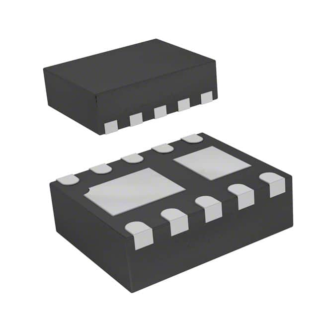
- Part No.:
- STBP120CVDK6F
- Manufacturer:
- STMicroelectronics
- Category:
- Power Management - Specialized
- Package:
- 10-WFDFN Exposed Pad
- Datasheet:
-
 STBP120CVDK6F.pdf
- Description:
- IC OVP W/THERMAL SHUTDOWN 10TDFN
- Quantity:
- Payment:

- Shipping:

Inventory:1,604
Please send an inquiry. Send us your inquiry, and we will respond immediately.
Product details
Overview
STBP120CVDK6F from STMicroelectronics is an overvoltage protection device featuring an integrated 90 mΩ N-channel MOSFET switch, thermal shutdown, soft-start, and active-low open-drain FLT output. It operates with input voltages up to +28 V, provides ±15 kV air-discharge ESD protection on IN, and complies with China YD/T 1591-2006 overvoltage requirements for portable power inputs in smartphones and digital cameras.
For engineers reviewing the STBP120CVDK6F datasheet, STBP120CVDK6F pinout, STBP120CVDK6F application, or STBP120CVDK6F equivalent, this device serves as a system-level input protection IC with precise OVLO/UVLO thresholds, junction temperature monitoring, and microcontroller-controllable enable/fault signaling - critical for USB-powered and battery-charging subsystems requiring robust fault isolation.
Technical Context
The STBP120CVDK6F implements a high-side N-channel MOSFET switch controlled by an internal charge pump, enabling operation from low VIN (≥3.25 V UVLO) while supporting up to 28 V input. Its protection logic combines analog voltage comparators for OVLO (typ. 6.4 V) and UVLO (typ. 3.25 V), plus a thermal sensor triggering shutdown at TJ ≥125 °C with 20 °C hysteresis.
Startup behavior includes two sequential 50 ms delays: ton (output turn-on after stable VIN) and tstart (FLT deactivation after output stabilization). The FLT pin remains functional regardless of EN state, and reverse current conduction (OUT→IN) is enabled via the MOSFET body diode - a deliberate topology for peripheral powering, though thermal shutdown does not protect against reverse-current-induced heating.
Key Specifications
| Parameter | Value and Actual Design Meaning |
|---|---|
| Input Voltage Range | +3.25 V to +28 V - UVLO enables operation only above 3.25 V; OVLO disables output above 6.4 V (typ.) to prevent downstream damage. |
| RDS(on) | 90 mΩ (typ.) at ID = 1 A - Enables <100 mV drop at 1 A, minimizing power loss and self-heating during normal conduction. |
| OVLO Threshold | 6.4 V (typ.), 6.2–6.6 V (min/max) - Matches USB OTG and legacy charger overvoltage limits; hysteresis improves noise immunity. |
| Thermal Shutdown | 125 °C (TOFF) with 20 °C hysteresis - Protects silicon integrity under sustained overload; recovery requires TJ ≤105 °C. |
| ESD Rating (IN) | ±15 kV (air), ±8 kV (contact) - Validated with 1 µF input capacitor; exceeds IEC 61000-4-2 Level 4 for system-level robustness. |
| Soft-Start Delay (ton) | 50 ms - Prevents inrush current surges into downstream capacitive loads during power-up or fault recovery. |
| FLT Output Type | Active-low open-drain - Allows wired-OR fault signaling across multiple protection devices; requires external pull-up (10 kΩ–1 MΩ). |
Pinout & Package
STBP120CVDK6F uses a RoHS-compliant TDFN-10 package (2.5 mm × 2.0 mm × 0.75 mm, 0.5 mm pitch) with exposed thermal pads (PAD1, PAD2) that may be tied to IN or GND for improved thermal performance or noise immunity.
| Pin/Terminal | Circuit Role | Design Meaning |
|---|---|---|
| IN (Pins 4, 5) | Input supply node | Accepts DC input up to 28 V; requires ≥1 µF low-ESR ceramic capacitor placed adjacent to pins for ESD and transient suppression. |
| OUT (Pins 6, 7) | Protected output node | Delivers regulated input voltage to load when enabled; supports bidirectional current flow (OUT→IN) via MOSFET body diode. |
| FLT (Pin 3) | Fault status indicator | Open-drain output pulled low during UVLO, OVLO, or thermal shutdown; remains active regardless of EN state. |
| EN (Pin 10) | Enable control input | Active-low logic input with no internal pull-down; must be driven or externally pulled to GND to activate device. |
| GND (Pin 2) | Reference ground | Primary return path for all currents; connects to PCB ground plane; thermal pad ties to GND for optimal heat dissipation. |
| NC (Pins 1, 8, 9; PAD1, PAD2) | No-connect terminals | Electrically isolated; PAD1/PAD2 may be soldered to IN or GND to enhance thermal conduction or reduce EMI coupling. |
Key Features
| Feature | Design Value |
|---|---|
| Integrated charge pump | Enables full enhancement of high-voltage N-channel MOSFET from low VIN (≥3.25 V), eliminating need for external gate driver or P-channel device. |
| Programmable fault reporting | FLT pin signals all three fault conditions (UVLO/OVLO/thermal) with defined timing delays, enabling deterministic system-level fault response. |
| Bidirectional current capability | MOSFET body diode allows OUT→IN current flow - supports use cases like powering USB peripherals from battery via system connector without added diodes. |
| Configurable enable interface | EN pin lacks internal pull-down, allowing flexible control by MCU GPIO or external resistor network - avoids unintended activation during boot. |
| System-level ESD hardening | ±15 kV air/±8 kV contact ESD rating validated in typical application circuit (with 1 µF IN cap), reducing need for external TVS diodes. |
Applications
| Smartphone Charging Interface | Digital Camera Power Management |
|---|---|
|
Use Scenario: USB wall adapter or car charger connected to smartphone mainboard, subject to voltage transients and ESD events. IC Role / Device Role / Timing Role: High-side overvoltage protector placed between input connector and PMIC/battery charger IC. Use Value: Blocks >6.4 V spikes before they reach sensitive charging circuitry; FLT alerts baseband processor of fault condition within 50 ms. |
Use Scenario: External power supply (e.g., AC adapter) feeding image sensor and processor subsystems in compact digital camera. IC Role / Device Role / Timing Role: Input rail supervisor ensuring stable 5 V delivery while rejecting overvoltage and overheating faults. Use Value: Prevents latch-up or permanent damage to CMOS image sensors during adapter hot-plug or regulator failure; soft-start eliminates flash-trigger timing jitter. |
| PDA System Protection | MP3 Player Battery Charging Path |
|
Use Scenario: Legacy PDA with dual-input power (USB + barrel jack) where inconsistent adapter quality risks overvoltage exposure. IC Role / Device Role / Timing Role: Single-point protection element upstream of system LDOs and application processor. Use Value: Guarantees compliance with YD/T 1591-2006 overvoltage limits; NC pins allow optional thermal pad grounding to sustain 1.5 A continuous load on 2-layer PCB. |
Use Scenario: Portable MP3 player accepting 5 V USB input to charge Li-ion battery via dedicated charger IC. IC Role / Device Role / Timing Role: Fault-isolating switch between USB port and charger IC input, with EN controlled by system MCU. Use Value: Enables software-initiated power disconnect during battery full-charge or thermal fault; FLT signal triggers LED warning without firmware polling. |
Equivalent & Alternatives
The following parts are listed as comparable options for similar overvoltage protection applications.
| Alternative Part | Technical Difference | Application Difference | Selection Advice |
|---|---|---|---|
| TUSB544RGET | USB 3.1 re-driver with integrated 5.5 V OVLO; no thermal shutdown or FLT output; RDS(on) not specified. | Designed for high-speed signal integrity, not power rail protection; lacks standalone fault signaling. | Select only if USB data path conditioning is required alongside basic overvoltage clamp. |
| TPD3S014RTER | USB port protector with 5.7 V OVLO, ±15 kV ESD, but uses external FET; no integrated MOSFET or thermal shutdown. | Requires external high-side switch and control logic; higher BOM count and board area. | Choose when discrete layout flexibility or higher current (>2 A) is needed beyond STBP120's 1.5 A capability. |
Compared with TUSB544RGET and TPD3S014RTER, STBP120CVDK6F uniquely integrates OVLO, thermal shutdown, soft-start, and fault indication in a single 2.5×2 mm package - delivering complete, autonomous input protection without external components or host intervention.
Availability
STBP120CVDK6F is available at Aetrix Electronics and suitable for smartphone charging interfaces, digital camera power management, and PDA system protection requiring stable component supply, long-term lifecycle support, and RoHS-compliant packaging.
Supply support for STBP120CVDK6F includes scheduled delivery planning, volume procurement assistance, BOM continuity management, traceable sourcing, and lifecycle availability coordination for OEM customers, industrial embedded developers, connected-device designers, and electronics production programs.
Manufacturer
STMicroelectronics is a global semiconductor leader headquartered in Geneva, Switzerland, designing and manufacturing analog, MEMS, power, and microcontroller solutions for automotive, industrial, and consumer markets.
The STBP120 series belongs to ST's system protection product line, engineered specifically for robust, low-footprint overvoltage and thermal fault isolation in portable USB-powered devices - emphasizing reliability, ESD resilience, and seamless integration with battery charging architectures.
FAQ
Does STBP120CVDK6F support reverse current flow (OUT to IN), and how is it implemented?
Yes - the device allows reverse current via the intrinsic body diode of its integrated N-channel MOSFET. When voltage appears at OUT exceeding IN by ~0.7 V, current flows from OUT to IN. The MOSFET then turns on (after 50 ms delay) if IN rises above UVLO, reducing forward drop. This feature enables powering peripherals from battery via system connector, but thermal shutdown does not monitor reverse-current heating.
What is the exact OVLO threshold, and is it adjustable?
The OVLO threshold is factory-trimmed to 6.4 V (typical), with min/max range of 6.2 V to 6.6 V per datasheet Table 5. It is not user-adjustable; no external resistor or capacitor modifies this value. Hysteresis of 100 mV (typ.) ensures noise immunity during transient overvoltage events.
How should the FLT pin be interfaced with a 3.3 V microcontroller GPIO?
Connect FLT (open-drain) to the MCU GPIO via a 10–100 kΩ pull-up resistor to 3.3 V. No level-shifting is needed. The pin sinks ≤10 µA when active (low); when inactive (Hi-Z), the GPIO reads high. Avoid direct connection without pull-up, as FLT floats in fault-clear state and cannot drive high actively.
Can STBP120CVDK6F be used with input voltages below 3.25 V?
No - the undervoltage lockout (UVLO) circuit disables the MOSFET switch until VIN exceeds 3.25 V (typ.). Below this, OUT remains disconnected and FLT is driven low (if VIN ≥1.2 V). Operation below 1.2 V is undefined; the device draws minimal current (<1 µA) but provides no protection or signaling.
STBP120CVDK6F Specifications
- Product attributes
- Attribute value
- Manufacturer:
- STMicroelectronics
- Series:
- -
- Package/Case:
- 10-WFDFN Exposed Pad
- Packaging:
- Tape & Reel (TR)
- Product Status:
- Active
- Applications:
- Overload Protection
- Current - Supply:
- 170µA
- Voltage - Supply:
- 1.2V ~ 28V
- Operating Temperature:
- -40°C ~ 85°C
- Grade:
- -
- Qualification:
- -
- Mounting Type:
- Surface Mount
- Supplier Device Package:
- 10-TDFN (2.5x2.0)
STBP120CVDK6F FAQ
1.How can I place an order for STBP120CVDK6F through Aetrix?
Please submit a Request for Quotation (RFQ) for STBP120CVDK6F on Aetrix. Our sales agent will provide a competitive quotation and guide you through the order confirmation once you accept the terms.
2.Are the price and stock information for STBP120CVDK6F reliable?
The price and inventory of STBP120CVDK6F are updated periodically and may fluctuate due to market conditions. Stock and pricing data are typically refreshed every 24 hours. Quotation validity for STBP120CVDK6F is usually 5 days.
3.What payment methods are accepted for STBP120CVDK6F?
We accept Wire Transfer, PayPal, Credit Card, Western Union, MoneyGram, and Escrow for STBP120CVDK6F transactions.
Note: Certain payment methods may incur a processing fee.
4.How is shipping managed for STBP120CVDK6F?
STBP120CVDK6F orders can be shipped via leading logistics carriers, including DHL, UPS, FedEx, TNT, or Registered Mail.
Once your STBP120CVDK6F order is processed, you will receive an email with the shipment details and tracking number.
Note: Tracking information may take up to 24 hours to appear. Express delivery typically takes 3–5 business days.
5.How can I obtain technical support or documentation for STBP120CVDK6F?
For technical support, including STBP120CVDK6F datasheets, pinout diagrams, or application guidance, please contact our engineering support team. They can provide detailed documentation and assistance for your STBP120CVDK6F requirements.
6.How does Aetrix verify that STBP120CVDK6F is sourced from the original manufacturer or authorized distributors?
All STBP120CVDK6F products on Aetrix are procured from qualified distributors and authorized channels. Our dedicated quality assurance team conducts strict verification, including traceability checks and, if necessary, third-party testing. This ensures that STBP120CVDK6F meets industry standards.
7.What is the process for return or replacement of STBP120CVDK6F?
All STBP120CVDK6F units undergo pre-shipment inspection (PSI). If there is an issue with STBP120CVDK6F, returns or replacements are accepted under the following conditions:
1.Quantity discrepancies, incorrect items, or visible external defects (such as breakage or corrosion), acknowledged by Aetrix.
2.The issue is reported within 90 days of delivery.
3.The STBP120CVDK6F part is unused and in its original packaging.
Return procedure for STBP120CVDK6F:
1.Submit a request within 90 days.
2.Obtain a Return Material Authorization (RMA) from Aetrix.
STBP120CVDK6F Tags

-
TPS2511DGNR
Texas Instruments

-
UTC2000/MG
Microchip Technology

-
TUSB320HAIRWBR
Texas Instruments

-
TPS61252DSGR
Texas Instruments

-
PI5USB30216CXUAEX
Diodes Incorporated

-
SN6501DBVR
Texas Instruments

-
CYPD3177-24LQXQT
Infineon Technologies
-
SN6501QDBVRQ1
Texas Instruments

-
STUSB1600AQTR
STMicroelectronics

-
SN6505BDBVR
Texas Instruments
-
SN6501DBVT
Texas Instruments

-
TPS65150PWPR
Texas Instruments
Tech Hub

A practical engineering and sourcing framework covering lifecycle verification, lifetime-buy calculations, replacement qualification, supplier checks and counterfeit-risk controls.

TTL and CMOS logic families differ in thresholds, loading, output drive, power and timing. This engineering guide compares 74HC and 74HCT, calculates noise margins and checks 3.3 V/5 V compatibility.

A practical engineering guide to 3.3V and 5V logic compatibility, input thresholds, resistor dividers, translator ICs, MOSFET level shifting, I2C pull-ups, timing limits and power-sequencing risks.

The 74HC595 uses push-pull logic outputs, while the TPIC6B595 uses 50 V open-drain DMOS sinks for higher-power loads. This guide compares timing, current limits, 3.3 V interfacing, load wiring, thermal…

The 74HC595 converts serial data into eight stable parallel outputs. This guide covers pin functions, shift and storage timing, OE and MR behavior, drive-current limits, cascading, voltage compatibilit…

A technical comparison of level-sensitive latches and edge-triggered flip-flops, covering timing windows, setup and hold limits, master–slave operation, time borrowing, race-through, HDL inference and…

A D latch stores one bit while Enable controls when data can pass. This reference covers gate-level operation, truth tables, transparency, setup and hold timing, LE versus OE, common ICs and practical …

An SR latch stores one bit through cross-coupled feedback. This engineering reference covers NOR and NAND implementations, truth tables, forbidden-state recovery, gated operation, switch debouncing, fa…

Latch circuits retain one bit through feedback. This technical reference covers SR and D latches, truth tables, transparency, timing limits, latch-versus-flip-flop behavior, applications and common log…

An engineering guide to LED driver operation, constant-current and constant-voltage outputs, linear and switching topologies, dimming, IC selection, calculations, replacement compatibility, and fault c…


