
 My Inquiry
 My Account


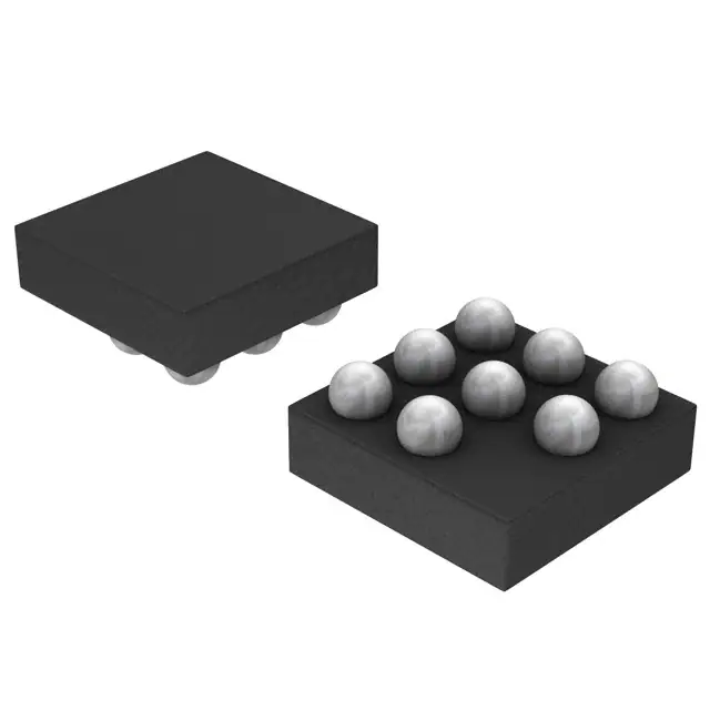
STMicroelectronics STPAC01F2
- Part No.:
- STPAC01F2
- Manufacturer:
- STMicroelectronics
- Category:
- RF Detectors
- Package:
- 8-WFBGA, FCBGA
- Datasheet:
-
 STPAC01F2.pdf
- Description:
- IC RF DETECT 800MHZ-1.9GHZ 8FLP
- Quantity:
- Payment:

- Shipping:

Inventory:4,750
Please send an inquiry. Send us your inquiry, and we will respond immediately.
Product details
Overview
STPAC01F2 from STMicroelectronics is a flip-chip RF power detector IC for cellular PA control, featuring dual DC outputs (VDCout and VTemp), 0.8–2 GHz operating frequency, ±0.09 V temperature-induced VDCout drift at 10 dBm, and 2.2–3.2 V bias voltage range. It enables closed-loop thermal compensation in GSM/DCS/PCS/CDMA handsets.
For engineers reviewing the STPAC01F2 datasheet, STPAC01F2 pinout, STPAC01F2 application, or STPAC01F2 equivalent, key selection criteria include its dual-output thermal compensation architecture, 50 µA bias current requirement, 8-bump flip-chip package, and RF detection accuracy across 800–1900 MHz bands with minimal frequency-dependent variation.
Technical Context
The STPAC01F2 integrates two matched diodes-one for RF-to-DC conversion, one for ambient temperature sensing-within a single flip-chip die. Its biasing stage cancels detection diode forward-voltage drift, enabling stable output under varying supply and temperature conditions.
It operates as a ratiometric detector: VDCout and VTemp track identically with temperature (ΔVDCout = ΔVTemp = 0.09 V over 0–70 °C), allowing differential amplification to reject thermal error. The device requires external 50 µA current sources on both outputs and supports coupler-based RF sampling in PA feedback loops.
Key Specifications
| Parameter | Value and Actual Design Meaning |
|---|---|
| Frequency Range | 0.8–2 GHz - Covers GSM850, DCS1800, PCS1900, AMPS, CDMA, TDMA bands |
| VDCout @ 10 dBm | 0.88 V (850 MHz), 1.07 V (1850 MHz) - Enables linear PA gain control mapping |
| VTemp Output | 1.93 V typ. at 25 °C - Matches VDCout thermal coefficient for ratiometric cancellation |
| Bias Voltage | 2.2–3.2 V - Low-voltage operation compatible with 3.3 V system rails |
| Temp Drift (ΔVDCout) | ±0.09 V over 0–70 °C - Specifies worst-case thermal error before compensation |
| ESD Rating | 250 V HBM - Sufficient for handheld assembly handling per MIL-STD-883E |
| Package | Flip Chip, 8 bumps, 1.57 × 1.57 mm - Enables ultra-low parasitic RF path for front-end integration |
Pinout & Package
STPAC01F2 uses an 8-bump flip-chip package (1.57 mm × 1.57 mm) with exposed thermal pad. Bumps are arranged in 3×3 grid with corner A1 marked by dot; Pin A1 = Gnd1, B1 = RFin, C1 = Gnd1, A2 = Gnd1, B2 = Gnd2, C2 = Bias, A3 = DC out, B3 = VTemp.
| Pin/Terminal | Circuit Role | Design Meaning |
|---|---|---|
| Gnd1 (A1, C1, A2) | RF ground reference | Three dedicated RF return paths minimize ground inductance for detector stability |
| RFin (B1) | RF input node | Direct connection to directional coupler output; no external matching required |
| Gnd2 (B2) | Analog ground reference | Separate low-noise return for bias and DC output circuitry |
| Bias (C2) | Bias voltage input | Supplies regulated current to internal diodes; must be 2.2–3.2 V |
| DC out (A3) | RF power detection output | Provides voltage proportional to coupled RF power; requires 50 µA sink |
| VTemp (B3) | Temperature sensing output | Provides voltage tracking die temperature; identical thermal coefficient to DC out |
Key Features
| Feature | Design Value |
|---|---|
| Dual-diode topology | Enables simultaneous RF power measurement and on-die temperature sensing with matched thermal coefficients |
| Zero-forward-drop biasing | Eliminates diode Vf drift impact on VDCout, improving accuracy across supply and temperature |
| Ratiometric output design | VDCout and VTemp exhibit identical ±0.09 V drift over 0–70 °C, enabling true thermal error cancellation |
| Flip-chip construction | Reduces parasitic inductance by >70% vs. wire-bonded equivalents, preserving RF linearity up to 2 GHz |
| ECOPACK® lead-free | Complies with JEDEC JESD97; second-level interconnect uses Pb-free solder bumps |
Applications
| GSM/DCS Handset PA Control | PCS/CDMA Mobile Transmitter |
|---|---|
Use Scenario: Closed-loop transmit power regulation in dual-band GSM/DCS phones using coupler-sampled RF feedback. IC Role / Device Role / Timing Role: RF detector providing VDCout for digital baseband power control loop; VTemp enables real-time thermal correction. Use Value: Maintains ±0.5 dB transmit power accuracy across –30 to +85 °C ambient, meeting 3GPP TR 25.943 requirements. | Use Scenario: Power amplifier output monitoring in PCS1900 and CDMA2000 mobile handsets operating at 1.85–1.99 GHz. IC Role / Device Role / Timing Role: High-frequency RF detector delivering temperature-compensated DC voltage to baseband ADC for PA gain calibration. Use Value: Delivers 1.07 V output at 10 dBm with <0.1 V thermal drift, enabling single-point calibration across full temperature range. |
| TDMA Base Station Front-End | Multi-Mode Cellular Module |
Use Scenario: RF power monitoring in TDMA infrastructure transceivers requiring stable detection up to 800 MHz. IC Role / Device Role / Timing Role: Low-drift RF detector interfacing with analog front-end ASIC; provides compensated DC signal for AGC loop. Use Value: Achieves 0.88 V output at 850 MHz with ±0.09 V tempco, reducing need for lookup-table compensation in FPGA-based control logic. | Use Scenario: Integrated PA control in compact multi-mode modules supporting GSM850/1900, DCS1800, and CDMA bands. IC Role / Device Role / Timing Role: Single-chip dual-output detector replacing discrete diode+thermistor solutions in space-constrained modules. Use Value: Saves ≥2.5 mm² PCB area and eliminates 3 passive components while maintaining ±0.3 dB power accuracy over temperature. |
Equivalent & Alternatives
The following parts are listed as comparable options for similar RF power detector applications.
| Alternative Part | Technical Difference | Application Difference | Selection Advice |
|---|---|---|---|
| MAX2016 | Single-output logarithmic detector; no integrated temperature sensor; 0.1–2.5 GHz range | Requires external thermistor and op-amp for thermal compensation | Preferred when board space allows discrete compensation and wider frequency coverage is needed |
| LT5537 | True RMS detector with internal temperature sensor but no ratiometric VTemp output; 0.1–1 GHz range | Delivers compensated output internally; no differential amplifier required | Selected when simplified signal chain (single output) outweighs need for 1.85 GHz performance |
Compared with MAX2016 and LT5537, STPAC01F2 uniquely delivers matched VDCout/VTemp outputs enabling hardware-level ratiometric cancellation-critical for high-accuracy PA control in compact handset designs where external compensation components are prohibitive.
Availability
STPAC01F2 is available at Aetrix Electronics and suitable for GSM/DCS handset design, PCS/CDMA mobile transmitter development, and TDMA base station front-end prototyping requiring stable component supply through extended production cycles.
Supply support for STPAC01F2 includes scheduled delivery planning, volume procurement assistance, BOM continuity management, traceable sourcing, and lifecycle availability coordination for OEM customers, industrial embedded developers, connected-device designers, and electronics production programs.
Manufacturer
STMicroelectronics is a global semiconductor leader headquartered in Geneva, designing and manufacturing analog, mixed-signal, power, and microcontroller products for automotive, industrial, and consumer markets.
The STPAC01F2 belongs to ST's IPAD™ RF front-end portfolio, engineered specifically for miniaturized, high-efficiency power amplifier control in cellular handsets and portable wireless devices.
FAQ
What is the required bias current for STPAC01F2 outputs?
The STPAC01F2 requires a precise 50 µA DC current sink on both VDCout and VTemp pins for accurate operation. This current must be supplied externally via precision current sources or high-impedance DACs; failure to maintain this load results in >5% output voltage error due to diode nonlinearity.
Can STPAC01F2 operate without thermal compensation?
Yes, STPAC01F2 can be used with only VDCout for basic RF detection, but uncorrected thermal drift exceeds ±0.44 V over the full bias range (2.2–3.2 V) and ±0.09 V over 0–70 °C ambient. Full accuracy requires connecting both outputs to a differential amplifier as shown in Figure 10.
What is the maximum RF input power rating?
The absolute maximum RF input power is +20 dBm (100 mW) per Absolute Ratings Table 1. Operation above +10 dBm degrades linearity and increases thermal self-heating effects; sustained operation above +15 dBm risks permanent damage to the detection diodes.
Is STPAC01F2 still in active production?
STPAC01F2 is marked as "Obsolete Product(s)" in the official ST datasheet revision history (Rev 2, April 2008). Aetrix Electronics maintains legacy inventory with full traceability and offers engineering support for end-of-life transition planning, including validated drop-in alternatives for ongoing production.
STPAC01F2 Specifications
- Product attributes
- Attribute value
- Manufacturer:
- STMicroelectronics
- Series:
- -
- Packaging:
- Tape & Reel (TR)
- Product Status:
- Obsolete
- Frequency:
- 800MHz ~ 1.9GHz
- RF Type:
- AMPS, CDMA, DCS, GSM, TDMA
- Input Range:
- -
- Accuracy:
- -
- Voltage - Supply:
- 2.2V ~ 3.2V
- Mounting Type:
- 500 µA
- Supplier Device Package:
- Surface Mount
- Current - Supply:
- 8-FlipChip (1.57x1.57)
STPAC01F2 FAQ
1.How can I place an order for STPAC01F2 through Aetrix?
Please submit a Request for Quotation (RFQ) for STPAC01F2 on Aetrix. Our sales agent will provide a competitive quotation and guide you through the order confirmation once you accept the terms.
2.Are the price and stock information for STPAC01F2 reliable?
The price and inventory of STPAC01F2 are updated periodically and may fluctuate due to market conditions. Stock and pricing data are typically refreshed every 24 hours. Quotation validity for STPAC01F2 is usually 5 days.
3.What payment methods are accepted for STPAC01F2?
We accept Wire Transfer, PayPal, Credit Card, Western Union, MoneyGram, and Escrow for STPAC01F2 transactions.
Note: Certain payment methods may incur a processing fee.
4.How is shipping managed for STPAC01F2?
STPAC01F2 orders can be shipped via leading logistics carriers, including DHL, UPS, FedEx, TNT, or Registered Mail.
Once your STPAC01F2 order is processed, you will receive an email with the shipment details and tracking number.
Note: Tracking information may take up to 24 hours to appear. Express delivery typically takes 3–5 business days.
5.How can I obtain technical support or documentation for STPAC01F2?
For technical support, including STPAC01F2 datasheets, pinout diagrams, or application guidance, please contact our engineering support team. They can provide detailed documentation and assistance for your STPAC01F2 requirements.
6.How does Aetrix verify that STPAC01F2 is sourced from the original manufacturer or authorized distributors?
All STPAC01F2 products on Aetrix are procured from qualified distributors and authorized channels. Our dedicated quality assurance team conducts strict verification, including traceability checks and, if necessary, third-party testing. This ensures that STPAC01F2 meets industry standards.
7.What is the process for return or replacement of STPAC01F2?
All STPAC01F2 units undergo pre-shipment inspection (PSI). If there is an issue with STPAC01F2, returns or replacements are accepted under the following conditions:
1.Quantity discrepancies, incorrect items, or visible external defects (such as breakage or corrosion), acknowledged by Aetrix.
2.The issue is reported within 90 days of delivery.
3.The STPAC01F2 part is unused and in its original packaging.
Return procedure for STPAC01F2:
1.Submit a request within 90 days.
2.Obtain a Return Material Authorization (RMA) from Aetrix.
STPAC01F2 Tags
-
LMH2110TMX/NOPB
Texas Instruments
-
MAX2204EXK+T
Analog Devices Inc./Maxim Integrated
-
LMV221SD/NOPB
Texas Instruments
-
LTC5505-2ES5#TRMPBF
Analog Devices Inc.
-
LTC5505-1ES5#TRMPBF
Analog Devices Inc.
-
AD8314ACPZ-RL7
Analog Devices Inc.
-
ADL5506ACBZ-R7
Analog Devices Inc.
-
AD8312ACBZ-P7
Analog Devices Inc.
-
MAX4003EUA+T
Analog Devices Inc./Maxim Integrated
-
LTC5530ES6#TRMPBF
Analog Devices Inc.
-
LTC5507ES6#TRMPBF
Analog Devices Inc.
-
LTC5507ES6#TRPBF
Analog Devices Inc.
Tech Hub

A practical engineering and sourcing framework covering lifecycle verification, lifetime-buy calculations, replacement qualification, supplier checks and counterfeit-risk controls.

TTL and CMOS logic families differ in thresholds, loading, output drive, power and timing. This engineering guide compares 74HC and 74HCT, calculates noise margins and checks 3.3 V/5 V compatibility.

A practical engineering guide to 3.3V and 5V logic compatibility, input thresholds, resistor dividers, translator ICs, MOSFET level shifting, I2C pull-ups, timing limits and power-sequencing risks.

The 74HC595 uses push-pull logic outputs, while the TPIC6B595 uses 50 V open-drain DMOS sinks for higher-power loads. This guide compares timing, current limits, 3.3 V interfacing, load wiring, thermal…

The 74HC595 converts serial data into eight stable parallel outputs. This guide covers pin functions, shift and storage timing, OE and MR behavior, drive-current limits, cascading, voltage compatibilit…

A technical comparison of level-sensitive latches and edge-triggered flip-flops, covering timing windows, setup and hold limits, master–slave operation, time borrowing, race-through, HDL inference and…

A D latch stores one bit while Enable controls when data can pass. This reference covers gate-level operation, truth tables, transparency, setup and hold timing, LE versus OE, common ICs and practical …

An SR latch stores one bit through cross-coupled feedback. This engineering reference covers NOR and NAND implementations, truth tables, forbidden-state recovery, gated operation, switch debouncing, fa…

Latch circuits retain one bit through feedback. This technical reference covers SR and D latches, truth tables, transparency, timing limits, latch-versus-flip-flop behavior, applications and common log…

An engineering guide to LED driver operation, constant-current and constant-voltage outputs, linear and switching topologies, dimming, IC selection, calculations, replacement compatibility, and fault c…


