
 My Inquiry
 My Account


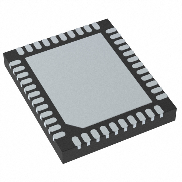
STMicroelectronics STPMIC1EPQR
- Part No.:
- STPMIC1EPQR
- Manufacturer:
- STMicroelectronics
- Category:
- Power Management - Specialized
- Package:
- 44-WFQFN Exposed Pad
- Datasheet:
-
 STPMIC1EPQR.pdf
- Description:
- 14 OUTPUT RAILS PMIC 4 ADJUSTABL
- Quantity:
- Payment:

- Shipping:

Inventory:14,886
Please send an inquiry. Send us your inquiry, and we will respond immediately.
Product details
Overview
STPMIC1EPQR from STMicroelectronics is a highly integrated power management IC (PMIC) designed as a companion chip for the STM32MP1 microprocessor unit. It delivers six LDOs-including DDR3 termination (sink-source), USB PHY, and reference voltage rails-four adaptive COT buck converters, a 5.2 V/1.1 A boost converter with bypass mode, two 500 mA power switches, and user-programmable NVM. It operates from 2.8 V to 5.5 V input and supports low-power wearable and IoT applications requiring precise rail sequencing and USB OTG compliance.
For engineers reviewing the STPMIC1EPQR datasheet, STPMIC1EPQR pinout, STPMIC1EPQR application, or STPMIC1EPQR equivalent, this page provides verified technical context, exact pin functions, real-world use cases in STM32MP1-based embedded systems, and validated alternative configurations aligned with DDR3L, lpDDR3, and USB PHY supply requirements.
Technical Context
The STPMIC1EPQR implements an I²C + digital IO control architecture with non-volatile memory (NVM) pre-programmed for STM32MP1E series compatibility-specifically configuring BUCK1 at 1.2 V (Rank3), BUCK3 at 1.8 V (Rank1), BUCK4 at 1.2 V (Rank2), LDO2 at 1.8 V (Rank0), and LDO5 at 2.9 V (Rank2). Its adaptive constant-on-time (COT) buck regulators feature integrated PLL synchronization for EMI reduction, while the LDO3 supports three modes: normal (1.8–3.3 V), sink-source (for DDR VTT at VOUT2/2), and bypass (low-drop RDS(on) = 0.45 Ω).
Thermal design is enabled by a WFQFN-44 package with exposed pad (EPGND), 7 °C/W junction-to-case thermal resistance, and operation up to 125 °C junction temperature. Power sequencing follows four programmable ranks (0–3), with automatic turn-on enabled for all rails except BOOST and switches-ensuring deterministic startup for multi-rail MPU systems without host intervention.
Key Specifications
| Parameter | Value and Actual Design Meaning |
|---|---|
| Input Voltage Range | 2.8 V to 5.5 V - supports single-cell Li-ion, USB 5 V, and industrial 3.3 V/5 V rails without external regulation. |
| Buck Converters | 4 × adaptive COT SMPS - each optimized for fast transient response, >90% peak efficiency, and PWM/PSM seamless transition. |
| Boost Converter | 5.2 V / 1.1 A with bypass mode - powers up to three USB ports (two 500 mA hosts + one 100 mA OTG) directly from battery or 5 V adapter. |
| LDO3 Functionality | Triple-mode: normal (1.8–3.3 V), sink-source (DDR3 VTT at VOUT2/2), or bypass (RDS(on) = 0.45 Ω) - eliminates need for external VTT termination circuitry. |
| NVM Configuration | Pre-programmed for STM32MP1E - defines default voltages, power-up sequence ranks, auto-turn-on behavior, and I²C slave address out-of-box. |
| Quiescent Current | 50 µA in OFF mode, 110 µA in STANDBY - enables ultra-low-power always-on system monitoring for wake-on-event designs. |
| Package | WFQFN-44 (5 mm × 6 mm × 0.8 mm) with exposed thermal pad - supports high-density PCB layouts and efficient heat dissipation in portable form factors. |
Pinout & Package
STPMIC1EPQR uses a WFQFN-44L (5 × 6 × 0.8 mm) package with exposed thermal pad (EPGND) requiring solder connection to PCB ground plane for thermal and electrical integrity.
| Pin/Terminal | Circuit Role | Design Meaning |
|---|---|---|
| RSTn (Pin 1) | Bi-directional reset | Active-low reset with internal pull-up; used for hardware-initiated recovery or safe power-down coordination. |
| WAKEUP (Pin 2) | Host wake signal | Active-high input enabling power-on from deep sleep via AP GPIO, supporting low-leakage standby states. |
| SDA / SCL (Pins 3–4) | I²C interface | Standard 1.8 V/3.3 V tolerant bus for dynamic voltage scaling, fault reporting, and NVM reprogramming in-system. |
| VOUT1–VOUT4 (Pins 5,9,31,27) | Buck feedback inputs | Resistive divider nodes for closed-loop output voltage regulation-enables precision ±2% accuracy across load/temperature. |
| VLX1–VLX4 / VLXBST (Pins 7,11,29,25,33) | Switch node connections | High-frequency LX nodes driving external inductors; require tight layout to minimize EMI and switching losses. |
| LDO3IN / LDO3OUT (Pins 13–14) | DDR VTT supply path | Supports sink-source operation for DDR3/DDR3L termination-dual-current capability (±120 mARMS) matches memory bus signaling needs. |
| VREFDDR (Pin 16) | DDR reference output | Provides VOUT2/2 (e.g., 0.675 V for 1.35 V DDR3L) with ±1% accuracy and 5 mARMS drive-critical for memory timing margin. |
| VIN (Pin 36) | Main power input | Primary 2.8–5.5 V source feeding LDO4, VREF, and all BUCKxIN pins-must be decoupled with ≥4.7 µF ceramic capacitor. |
| SWIN / SWOUT (Pins 37–38) | USB OTG switch path | 500 mA USB OTG-compliant power switch with overcurrent protection-enables bidirectional VBUS control per USB 2.0 spec. |
| INTn (Pin 43) | Interrupt output | Open-drain active-low signal indicating faults (OVP/OCP/thermal warning), sequencer completion, or regulator ready status. |
Key Features
| Feature | Design Value |
|---|---|
| Adaptive COT buck control | Enables <10 µs OCP response and <1% output deviation during 10–90% load steps-critical for CPU core voltage stability. |
| Triple-mode LDO3 | Eliminates discrete DDR termination components: sink-source mode delivers matched ±120 mARMS current; bypass mode reduces dropout to 0.45 Ω. |
| Programmable power sequencing | Four-rank (0–3) startup with configurable delay (7/10/13 ms) ensures correct voltage ramp order for STM32MP1 core, DDR, and peripherals. |
| Integrated USB power management | Single-chip solution for dual 500 mA USB host ports + 100 mA OTG-includes automatic VBUS source detection and boost bypass for battery input. |
| User NVM configuration | Factory-programmed for STM32MP1E compatibility; supports field updates via I²C to adapt to custom rail requirements or new processor variants. |
Applications
| STM32MP1-Based Industrial HMI | Wearable Health Monitor |
|---|---|
|
Use Scenario: Touchscreen-enabled human-machine interface with dual-display output, CAN bus, and real-time Linux OS on STM32MP157. IC Role / Device Role / Timing Role: PMIC supplies VDD_CORE (1.2 V), VDD_DDR (1.35 V), VDD_USB (3.3 V), and DDR VTT (0.675 V) with synchronized startup and dynamic voltage scaling. Use Value: Eliminates 12 discrete regulators and sequencing logic; reduces BOM count by 65% while meeting DDR3L timing margins (tVAC ≤ 0.5 ns). |
Use Scenario: Compact ECG patch with Bluetooth LE, optical sensor, and rechargeable coin cell powering STM32WB55 MCU + analog front-end. IC Role / Device Role / Timing Role: Manages ultra-low-power states (50 µA OFF, 110 µA STANDBY), powers sensor bias rails (1.8 V, 2.9 V), and enables wake-on-ECG-event via WAKEUP pin. Use Value: Extends battery life to >7 days continuous operation; LDO6 (1.0 V @ 150 mA) cleanly powers RF transceiver without coupling noise into analog signal chain. |
| Smart Home Gateway | Portable Barcode Scanner |
|
Use Scenario: Wi-Fi 6 + Zigbee gateway running OpenWrt on STM32MP135, interfacing with multiple sensors and actuators. IC Role / Device Role / Timing Role: Delivers isolated 3.3 V (LDO4), 1.8 V (LDO1/LDO2), and 2.9 V (LDO5) rails for Ethernet PHY, flash memory, and SD card-each with independent enable/control. Use Value: PSRR >40 dB up to 100 kHz suppresses switching noise from buck converters, preventing packet loss in 100 Mbps Ethernet link. |
Use Scenario: Handheld laser scanner using STM32G0B1 MCU, CMOS imager, and USB-C host interface-requires robust 5 V USB OTG and 3.3 V logic supply. IC Role / Device Role / Timing Role: BOOST converter (5.2 V/1.1 A) powers USB-C VBUS; SWOUT (500 mA) drives laser diode driver; LDO4 (3.3 V/50 mA) supplies image sensor I/O. Use Value: Bypass mode allows direct battery-to-USB conversion during charging-reducing thermal stress and enabling 10,000+ scan cycles per charge. |
Equivalent & Alternatives
The following parts are listed as comparable options for similar PMIC applications.
| Alternative Part | Technical Difference | Application Difference | Selection Advice |
|---|---|---|---|
| STPMIC1APQR | Default BUCK1 = 1.2 V (Rank2), BUCK3 = 3.3 V (Rank1), LDO2 = 1.8 V (Rank0) - optimized for STM32MP1A base configuration. | Targets entry-level STM32MP151/153 designs with simpler DDR3L and fewer peripheral rails. | Select when using STM32MP151A/D with fixed 3.3 V auxiliary supply and no lpDDR3 support. |
| STPMIC1DPQR | Default BUCK1 = 1.2 V (Rank3), BUCK3 = 3.3 V (Rank1), LDO5 = 3.3 V (Rank2) - supports higher-voltage peripherals and dual-SD card interfaces. | Designed for STM32MP157D with dual-camera ISP and PCIe root complex requiring 3.3 V I/O and VREF. | Choose for designs needing 3.3 V LDO5 output and enhanced BUCK3 sequencing for high-speed interface power domains. |
Compared with STPMIC1EPQR, the APQR variant offers earlier BUCK1 activation (Rank2 vs Rank3) but lacks lpDDR3-optimized BUCK3 timing; the DPQR variant provides higher LDO5 voltage (3.3 V vs 2.9 V) at the cost of reduced flexibility for low-voltage memory interfaces.
Availability
STPMIC1EPQR is available at Aetrix Electronics and suitable for STM32MP1-based industrial HMIs, wearable health monitors, and smart home gateways requiring stable component supply, long-term lifecycle support, and guaranteed traceability.
Supply support for STPMIC1EPQR includes scheduled delivery planning, volume procurement assistance, BOM continuity management, traceable sourcing, and lifecycle availability coordination for OEM customers, industrial embedded developers, connected-device designers, and electronics production programs.
Manufacturer
STMicroelectronics is a global semiconductor leader headquartered in Geneva, Switzerland, specializing in microcontrollers, power management, sensors, and automotive ICs with vertical manufacturing and broad IP portfolio.
The STPMIC1 product line delivers fully integrated, NVM-configurable PMICs targeting high-performance application processors-designed specifically to simplify power architecture for STM32MP1 series MPUs in resource-constrained embedded systems.
FAQ
What is the default power-up sequence rank configuration for STPMIC1EPQR?
STPMIC1EPQR is factory-programmed with BUCK1 at Rank3 (13 ms delay), BUCK2 at Rank0 (no auto-on), BUCK3 at Rank1 (7 ms), BUCK4 at Rank2 (10 ms), LDO1–LDO6 at Rank0, and LDO3 enabled in normal mode. This sequence aligns with STM32MP157E's core-first, DDR-second boot flow and avoids voltage back-feeding during startup.
Can STPMIC1EPQR support lpDDR3 memory termination?
Yes-STPMIC1EPQR's LDO3 supports sink-source mode with ±120 mARMS current and programmable VOUT = VOUT2/2, enabling precise lpDDR3 VTT termination at 0.675 V (for 1.35 V VDDQ). The REFDDR output provides matching 0.675 V reference with ±1% accuracy and 5 mARMS drive, satisfying JEDEC JESD209-3 timing requirements.
How does the BOOST converter handle battery input below 5 V?
The BOOST converter enters bypass mode when VIN drops below ~4.2 V, routing battery voltage directly to BSTOUT and VBUSOTG with minimal dropout (RDS(on) ≈ 45 mΩ). This maintains USB OTG functionality down to 3.0 V battery voltage while disabling switching operation-reducing quiescent current to 20 µA and eliminating inductor losses.
Is NVM reprogramming supported in the field for STPMIC1EPQR?
Yes-STPMIC1EPQR supports full NVM reconfiguration via standard I²C commands (per DS12792 Section 5.3), including output voltage, power-up rank, OCP thresholds, and watchdog settings. Reprogramming requires no special voltage or timing sequences and can be performed live during system operation without reset.
STPMIC1EPQR Specifications
- Product attributes
- Attribute value
- Manufacturer:
- STMicroelectronics
- Series:
- -
- Package/Case:
- 44-WFQFN Exposed Pad
- Packaging:
- Tape & Reel (TR)
- Product Status:
- Active
- Applications:
- General Purpose
- Current - Supply:
- 1.2mA
- Voltage - Supply:
- 2.8V ~ 5.5V
- Operating Temperature:
- -40°C ~ 105°C (TA)
- Grade:
- -
- Qualification:
- -
- Mounting Type:
- Surface Mount
- Supplier Device Package:
- 44-WFQFN (5x6)
STPMIC1EPQR FAQ
1.How can I place an order for STPMIC1EPQR through Aetrix?
Please submit a Request for Quotation (RFQ) for STPMIC1EPQR on Aetrix. Our sales agent will provide a competitive quotation and guide you through the order confirmation once you accept the terms.
2.Are the price and stock information for STPMIC1EPQR reliable?
The price and inventory of STPMIC1EPQR are updated periodically and may fluctuate due to market conditions. Stock and pricing data are typically refreshed every 24 hours. Quotation validity for STPMIC1EPQR is usually 5 days.
3.What payment methods are accepted for STPMIC1EPQR?
We accept Wire Transfer, PayPal, Credit Card, Western Union, MoneyGram, and Escrow for STPMIC1EPQR transactions.
Note: Certain payment methods may incur a processing fee.
4.How is shipping managed for STPMIC1EPQR?
STPMIC1EPQR orders can be shipped via leading logistics carriers, including DHL, UPS, FedEx, TNT, or Registered Mail.
Once your STPMIC1EPQR order is processed, you will receive an email with the shipment details and tracking number.
Note: Tracking information may take up to 24 hours to appear. Express delivery typically takes 3–5 business days.
5.How can I obtain technical support or documentation for STPMIC1EPQR?
For technical support, including STPMIC1EPQR datasheets, pinout diagrams, or application guidance, please contact our engineering support team. They can provide detailed documentation and assistance for your STPMIC1EPQR requirements.
6.How does Aetrix verify that STPMIC1EPQR is sourced from the original manufacturer or authorized distributors?
All STPMIC1EPQR products on Aetrix are procured from qualified distributors and authorized channels. Our dedicated quality assurance team conducts strict verification, including traceability checks and, if necessary, third-party testing. This ensures that STPMIC1EPQR meets industry standards.
7.What is the process for return or replacement of STPMIC1EPQR?
All STPMIC1EPQR units undergo pre-shipment inspection (PSI). If there is an issue with STPMIC1EPQR, returns or replacements are accepted under the following conditions:
1.Quantity discrepancies, incorrect items, or visible external defects (such as breakage or corrosion), acknowledged by Aetrix.
2.The issue is reported within 90 days of delivery.
3.The STPMIC1EPQR part is unused and in its original packaging.
Return procedure for STPMIC1EPQR:
1.Submit a request within 90 days.
2.Obtain a Return Material Authorization (RMA) from Aetrix.
STPMIC1EPQR Tags

-
TPS2511DGNR
Texas Instruments

-
UTC2000/MG
Microchip Technology

-
TUSB320HAIRWBR
Texas Instruments

-
TPS61252DSGR
Texas Instruments

-
PI5USB30216CXUAEX
Diodes Incorporated

-
SN6501DBVR
Texas Instruments

-
CYPD3177-24LQXQT
Infineon Technologies
-
SN6501QDBVRQ1
Texas Instruments

-
STUSB1600AQTR
STMicroelectronics

-
SN6505BDBVR
Texas Instruments
-
SN6501DBVT
Texas Instruments

-
TPS65150PWPR
Texas Instruments
Tech Hub

A practical engineering and sourcing framework covering lifecycle verification, lifetime-buy calculations, replacement qualification, supplier checks and counterfeit-risk controls.

TTL and CMOS logic families differ in thresholds, loading, output drive, power and timing. This engineering guide compares 74HC and 74HCT, calculates noise margins and checks 3.3 V/5 V compatibility.

A practical engineering guide to 3.3V and 5V logic compatibility, input thresholds, resistor dividers, translator ICs, MOSFET level shifting, I2C pull-ups, timing limits and power-sequencing risks.

The 74HC595 uses push-pull logic outputs, while the TPIC6B595 uses 50 V open-drain DMOS sinks for higher-power loads. This guide compares timing, current limits, 3.3 V interfacing, load wiring, thermal…

The 74HC595 converts serial data into eight stable parallel outputs. This guide covers pin functions, shift and storage timing, OE and MR behavior, drive-current limits, cascading, voltage compatibilit…

A technical comparison of level-sensitive latches and edge-triggered flip-flops, covering timing windows, setup and hold limits, master–slave operation, time borrowing, race-through, HDL inference and…

A D latch stores one bit while Enable controls when data can pass. This reference covers gate-level operation, truth tables, transparency, setup and hold timing, LE versus OE, common ICs and practical …

An SR latch stores one bit through cross-coupled feedback. This engineering reference covers NOR and NAND implementations, truth tables, forbidden-state recovery, gated operation, switch debouncing, fa…

Latch circuits retain one bit through feedback. This technical reference covers SR and D latches, truth tables, transparency, timing limits, latch-versus-flip-flop behavior, applications and common log…

An engineering guide to LED driver operation, constant-current and constant-voltage outputs, linear and switching topologies, dimming, IC selection, calculations, replacement compatibility, and fault c…


