
 My Inquiry
 My Account


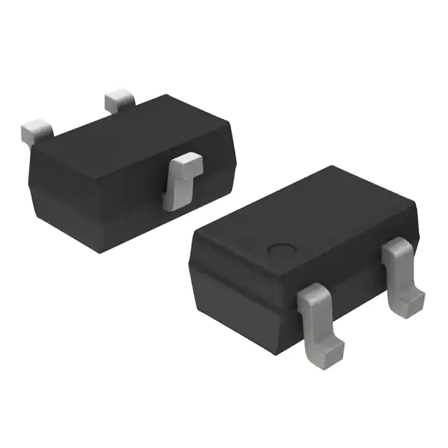
STMicroelectronics STPS60A150CS1

- Part No.:
- STPS60A150CS1
- Manufacturer:
- STMicroelectronics
- Category:
- Diode Arrays
- Package:
- TO-276AA
- Datasheet:
-
 STPS60A150CS1.pdf
- Description:
- DIODE ARRAY SCHOTT 150V 30A SMD5
- Quantity:
- Payment:

- Shipping:

Inventory:2
Please send an inquiry. Send us your inquiry, and we will respond immediately.
Product details
Overview
STPS60A150CS1 from STMicroelectronics is a radiation-hardened, dual common-cathode Schottky rectifier in a hermetic SMD.5 surface-mount package, rated for 2 × 30 A average forward current per diode and 150 V repetitive peak reverse voltage, with max forward voltage of 0.83 V at 30 A/125 °C - deployed in satellite power conversion stages requiring TID immunity up to 3 Mrad(Si) and SEB resistance under high-LET irradiation.
For engineers reviewing the STPS60A150CS1 datasheet, STPS60A150CS1 pinout, STPS60A150CS1 application, or STPS60A150CS1 equivalent, this part supports critical DC-DC converter output rectification, EPC (Electric Power Controller) secondary-side conduction, and radiation-tolerant PFC front-end designs where low VF, dV/dt immunity (10 kV/µs), and ESCC 5106/023 compliance are mandatory selection criteria.
Technical Context
This monolithic dual-die Schottky rectifier integrates two independent 30 A diodes sharing a common cathode terminal in a single SMD.5 ceramic/metal hermetic package. Its design eliminates parasitic inductance between dies and enables synchronized switching in high-reliability dual-phase outputs.
Characterized per ESCC 22900 (TID) and ESCC 25100 (SEE), it sustains full electrical performance after 3 Mrad(Si) exposure and shows no Single Event Burnout up to LET = 62.5 MeV·cm²/mg at ≤100% VRmax - verified across unbiased, forward-biased, and reverse-biased bias conditions during irradiation.
Key Specifications
| Parameter | Value and Actual Design Meaning |
|---|---|
| IF(AV) | 2 × 30 A - dual-diode rating enables parallel-output or interleaved converter topologies without external current-sharing components |
| VRRM | 150 V - supports 100 V nominal bus systems with 50% safety margin against transients in LEO/MEO satellite power rails |
| VF(max) | 0.83 V @ 30 A / 125 °C - reduces conduction loss by ≥25% vs. comparable Si fast recovery diodes, lowering thermal load in sealed modules |
| dV/dt | 10 kV/µs - prevents spurious turn-on during fast-switching GaN/SiC inverter transitions in motor drive or EPS subsystems |
| Rth(j-c) | 3.4 °C/W per diode - enables direct mounting to aluminum chassis without heatsink, simplifying thermal design in volume-constrained avionics enclosures |
| Tj(max) | +175 °C - allows operation in uncooled zones near propulsion electronics or solar array regulators where ambient exceeds 125 °C |
| Rad-Hard Qual | ESCC 5106/023 - flight-model qualified with full traceability, wafer-lot-level TID/SEE data, and serial-numbered certificates of conformance |
Pinout & Package
The STPS60A150CS1 uses the SMD.5 hermetic surface-mount package: ceramic base with metal lid, gold-plated terminations, 1 g mass, and 3-terminal configuration (Anode1, Anode2, Common Cathode). The top metallic lid is electrically isolated from all die and terminals.
| Pin/Terminal | Circuit Role | Design Meaning |
|---|---|---|
| 1 (Anode A) | First diode anode | Connects to primary switching node of first phase; supports independent gate-drive referencing in dual-phase synchronous rectifiers |
| 2 (Anode B) | Second diode anode | Connects to second-phase switching node; matched thermal and electrical characteristics ensure balanced current sharing between dies |
| 3 (Cathode) | Common cathode | Single low-inductance return path for both diodes; minimizes ground bounce in high-di/dt aerospace converters |
Key Features
| Feature | Design Value |
|---|---|
| Monolithic dual die | Two matched Schottky junctions on one silicon substrate - eliminates inter-device parameter spread and ensures <±2% VF mismatch at 30 A |
| Hermetic SMD.5 package | Sealed ceramic/metal construction - achieves MIL-STD-883 Class H reliability and prevents moisture-induced parametric drift in vacuum or humid launch environments |
| TID immunity | 3 Mrad(Si) total ionizing dose tolerance - validated across bias states with zero parameter shift beyond spec limits post-irradiation and annealing |
| SEB resistance | No burnout observed at LET = 62.5 MeV·cm²/mg up to 100% VRmax - enables use in outer Van Allen belt orbits without derating |
| ESCC qualification | Complies fully with ESCC 5106/023/02 - includes wafer-lot traceability, 100% screening, and flight-model documentation per ESA requirements |
Applications
| Satellite Power Converter Output Stage | Electric Propulsion Control Unit (EPC) |
|---|---|
|
Use Scenario: Final-stage rectification in 28 V or 100 V regulated bus converters supplying payload instruments and attitude control systems. IC Role / Device Role / Timing Role: Dual-phase synchronous rectifier replacing discrete Si diodes to reduce losses and improve efficiency in 300–500 kHz LLC resonant converters. Use Value: 0.83 V VF at 30 A/125 °C cuts conduction loss by 1.8 W per diode vs. legacy Si FRDs, enabling passive cooling in radiation-shielded compartments. |
Use Scenario: High-current output rectification in Hall-effect thruster power processing units operating continuously for >10,000 hours. IC Role / Device Role / Timing Role: Common-cathode dual Schottky handling bidirectional energy flow during regenerative braking and thrust modulation cycles. Use Value: 10 kV/µs dV/dt rating prevents false triggering during rapid polarity reversal in pulsed plasma discharge events. |
| Solar Array Regulator Secondary Side | Onboard Computer Power Sequencing |
|
Use Scenario: MPPT output rectification feeding battery charge controllers in geostationary telecom satellites exposed to 15-year cumulative TID. IC Role / Device Role / Timing Role: Radiation-hardened rectifier ensuring uninterrupted power delivery despite cumulative 3 Mrad(Si) exposure over mission lifetime. Use Value: Full ESCC 5106/023 qualification guarantees zero parameter degradation after end-of-life TID dose, eliminating need for derating. |
Use Scenario: Controlled power-up sequencing for multi-rail FPGAs and rad-hard microcontrollers in command & data handling units. IC Role / Device Role / Timing Role: Low-VF dual rectifier isolating auxiliary rails during cold-start, preventing backfeed into main 3.3 V/1.2 V domains. Use Value: Matched VF between dies (<±2%) ensures simultaneous turn-on, avoiding rail collapse during simultaneous FPGA core/I/O power ramp. |
Equivalent & Alternatives
The following parts are listed as comparable options for similar dual Schottky rectifier applications.
| Alternative Part | Technical Difference | Application Difference | Selection Advice |
|---|---|---|---|
| VMI S150D20 | Same 150 V VRRM and dual-common-cathode topology, but rated for 2 × 20 A; lower Tj(max) = +150 °C; not ESCC-qualified | Acceptable for non-flight engineering models or terrestrial test benches where radiation hardness is not required | Select only for prototyping or ground-support equipment where full ESCC traceability and 3 Mrad(Si) validation are unnecessary |
| IXYS DSSK60-015A | Higher IF(AV) = 2 × 40 A, but TO-263 package (non-hermetic); no TID/SEE characterization; VF = 0.92 V @ 30 A/125 °C | Suitable for high-power industrial UPS or EV chargers, but unsuitable for space due to lack of radiation testing and packaging | Choose only for cost-sensitive, non-radiation environments where thermal performance outweighs hermeticity and qualification rigor |
Compared with VMI S150D20 and IXYS DSSK60-015A, STPS60A150CS1 uniquely delivers flight-grade ESCC 5106/023 qualification, hermetic SMD.5 packaging, and validated 3 Mrad(Si) immunity - making it the sole option for mission-critical LEO/MEO satellite power systems requiring zero-failure reliability.
Availability
STPS60A150CS1 is available at Aetrix Electronics and suitable for satellite power converter output stages, electric propulsion control units, and solar array regulator secondary sides requiring stable component supply with full ESCC traceability and radiation-hardness assurance.
Supply support for STPS60A150CS1 includes scheduled delivery planning, volume procurement assistance, BOM continuity management, traceable sourcing, and lifecycle availability coordination for OEM customers, industrial embedded developers, connected-device designers, and electronics production programs.
Manufacturer
STMicroelectronics is a global semiconductor leader headquartered in Geneva, Switzerland, designing and manufacturing automotive, industrial, and aerospace-grade ICs and discrete devices with vertical fabrication capability.
This device belongs to ST's Rad-Hard Discrete portfolio, engineered specifically for space-grade power conversion where radiation tolerance, hermetic reliability, and ESCC-compliant documentation are non-negotiable system requirements.
FAQ
What is the difference between STPS60A150CS1 and STPS60A150CSG?
STPS60A150CS1 is the engineering model (design model) with gold-plated terminations and strip-pack packaging; STPS60A150CSG is the flight model qualified to ESCC 5106/023/02 with full lot traceability, wafer-level radiation test reports, and serialization. Both share identical electrical and thermal specs, but only the CSG variant carries flight certification.
Is the SMD.5 package lead-free and RoHS-compliant?
Yes - the SMD.5 package uses gold-plated terminations and complies with RoHS Directive 2011/65/EU. ST confirms full exemption from lead-based solder requirements per ECOPACK2 specifications, and the 1 g mass includes no restricted substances above threshold limits.
Can STPS60A150CS1 be used in zero-bias or reverse-biased TID testing configurations?
Yes - per DS12256 Rev 7 Section 2.1, the device was characterized under three bias conditions: unbiased, forward-biased, and reverse-biased, all at high dose rate. Performance remained within specification across all configurations after 3 Mrad(Si), confirming robustness in standby, conduction, and blocking states.
Does the common cathode configuration support independent thermal monitoring of each diode?
No - the monolithic dual die shares a single thermal path to the case; Rth(j-c) is specified per diode (3.4 °C/W) but measured from junction to common case surface. Independent thermal sensing requires external thermistors mounted adjacent to each anode pad, as no internal thermal sensors or separate cathode thermal vias are provided.
STPS60A150CS1 Specifications
- Product attributes
- Attribute value
- Manufacturer:
- STMicroelectronics
- Series:
- -
- Package/Case:
- TO-276AA
- Packaging:
- Strip
- Product Status:
- Active
- Diode Configuration:
- 1 Pair Common Cathode
- Technology:
- Schottky
- Voltage - DC Reverse (Vr) (Max):
- 150 V
- Current - Average Rectified (Io) (per Diode):
- 30A
- Voltage - Forward (Vf) (Max) @ If:
- 990 mV @ 30 A
- Speed:
- Fast Recovery =< 500ns, > 200mA (Io)
- Reverse Recovery Time (trr):
- -
- Current - Reverse Leakage @ Vr:
- 14 µA @ 150 V
- Operating Temperature - Junction:
- 175°C
- Grade:
- -
- Qualification:
- -
- Mounting Type:
- Surface Mount
- Supplier Device Package:
- SMD5
STPS60A150CS1 FAQ
1.How can I place an order for STPS60A150CS1 through Aetrix?
Please submit a Request for Quotation (RFQ) for STPS60A150CS1 on Aetrix. Our sales agent will provide a competitive quotation and guide you through the order confirmation once you accept the terms.
2.Are the price and stock information for STPS60A150CS1 reliable?
The price and inventory of STPS60A150CS1 are updated periodically and may fluctuate due to market conditions. Stock and pricing data are typically refreshed every 24 hours. Quotation validity for STPS60A150CS1 is usually 5 days.
3.What payment methods are accepted for STPS60A150CS1?
We accept Wire Transfer, PayPal, Credit Card, Western Union, MoneyGram, and Escrow for STPS60A150CS1 transactions.
Note: Certain payment methods may incur a processing fee.
4.How is shipping managed for STPS60A150CS1?
STPS60A150CS1 orders can be shipped via leading logistics carriers, including DHL, UPS, FedEx, TNT, or Registered Mail.
Once your STPS60A150CS1 order is processed, you will receive an email with the shipment details and tracking number.
Note: Tracking information may take up to 24 hours to appear. Express delivery typically takes 3–5 business days.
5.How can I obtain technical support or documentation for STPS60A150CS1?
For technical support, including STPS60A150CS1 datasheets, pinout diagrams, or application guidance, please contact our engineering support team. They can provide detailed documentation and assistance for your STPS60A150CS1 requirements.
6.How does Aetrix verify that STPS60A150CS1 is sourced from the original manufacturer or authorized distributors?
All STPS60A150CS1 products on Aetrix are procured from qualified distributors and authorized channels. Our dedicated quality assurance team conducts strict verification, including traceability checks and, if necessary, third-party testing. This ensures that STPS60A150CS1 meets industry standards.
7.What is the process for return or replacement of STPS60A150CS1?
All STPS60A150CS1 units undergo pre-shipment inspection (PSI). If there is an issue with STPS60A150CS1, returns or replacements are accepted under the following conditions:
1.Quantity discrepancies, incorrect items, or visible external defects (such as breakage or corrosion), acknowledged by Aetrix.
2.The issue is reported within 90 days of delivery.
3.The STPS60A150CS1 part is unused and in its original packaging.
Return procedure for STPS60A150CS1:
1.Submit a request within 90 days.
2.Obtain a Return Material Authorization (RMA) from Aetrix.
STPS60A150CS1 Tags
-
BAV99-7-F
Diodes Incorporated
-
BAT54C-7-F
Diodes Incorporated
-
BAV99,215
Nexperia USA Inc.
-
BAT54SLT1G
onsemi
-
BAV70LT1G
onsemi
-
BAT54CLT1G
onsemi
-
BAT54S-7-F
Diodes Incorporated
-
BAV99LT1G
onsemi
-
BAT54S,215
Nexperia USA Inc.
-
BAS40-04LT1G
onsemi
-
MMBD1503-TP
Micro Commercial Co
-
BAV99WT1G
onsemi
Tech Hub

A practical engineering guide to 3.3V and 5V logic compatibility, input thresholds, resistor dividers, translator ICs, MOSFET level shifting, I2C pull-ups, timing limits and power-sequencing risks.

The 74HC595 uses push-pull logic outputs, while the TPIC6B595 uses 50 V open-drain DMOS sinks for higher-power loads. This guide compares timing, current limits, 3.3 V interfacing, load wiring, thermal…

The 74HC595 converts serial data into eight stable parallel outputs. This guide covers pin functions, shift and storage timing, OE and MR behavior, drive-current limits, cascading, voltage compatibilit…

A technical comparison of level-sensitive latches and edge-triggered flip-flops, covering timing windows, setup and hold limits, master–slave operation, time borrowing, race-through, HDL inference and…

A D latch stores one bit while Enable controls when data can pass. This reference covers gate-level operation, truth tables, transparency, setup and hold timing, LE versus OE, common ICs and practical …

An SR latch stores one bit through cross-coupled feedback. This engineering reference covers NOR and NAND implementations, truth tables, forbidden-state recovery, gated operation, switch debouncing, fa…

Latch circuits retain one bit through feedback. This technical reference covers SR and D latches, truth tables, transparency, timing limits, latch-versus-flip-flop behavior, applications and common log…

An engineering guide to LED driver operation, constant-current and constant-voltage outputs, linear and switching topologies, dimming, IC selection, calculations, replacement compatibility, and fault c…

Operational amplifier guide covering op amp basics, feedback, ideal vs real op amps, common configurations, buffer circuits, offset, bias current, gain-bandwidth, slew rate, rail-to-rail limits and sel…

Jumper cables guide covering safe connection order, red and black clamp placement, final ground connection, cable gauge, length, clamp quality, copper vs CCA cables, jump starter comparison and battery…


