
 My Inquiry
 My Account


STMicroelectronics STWLC03JR
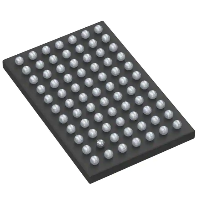
- Part No.:
- STWLC03JR
- Manufacturer:
- STMicroelectronics
- Category:
- Power Management - Specialized
- Package:
- 77-UFBGA, FCBGA
- Datasheet:
-
 STWLC03JR.pdf
- Description:
- IC WIRELESS POWER RECEIVER
- Quantity:
- Payment:

- Shipping:

Inventory:446
Please send an inquiry. Send us your inquiry, and we will respond immediately.
Product details
Overview
STWLC03JR from STMicroelectronics is a dual-mode Qi 1.1/PMA wireless power receiver IC with integrated synchronous rectifier, 800 kHz step-down converter, and 32-bit 16 MHz microcontroller (16 kB ROM / 2 kB RAM). It delivers up to 12 W output power with ≤90% DC-DC efficiency, supports configurable CC/CV battery charging or regulated 5 V supply mode, and includes I²C interface, NVM customization, and Rx coil NTC thermal protection - deployed in smartphones, power banks, and medical handheld devices.
For engineers reviewing the STWLC03JR datasheet, STWLC03JR pinout, STWLC03JR application, or STWLC03JR equivalent, key selection criteria include dual-standard protocol auto-detection, precise received power calculation via integrated ADCs, external supply switch control capability, programmable input voltage/current regulation loops, and flip-chip package thermal performance for compact wireless charging receivers.
Technical Context
The STWLC03JR implements digital control of both Qi and PMA communication stacks using its embedded 32-bit MCU, enabling autonomous standard detection and handshake without host intervention. Its analog control loops regulate rectified input voltage (VRECT) and current (IRECT) in real time to maintain stable power delivery under variable coupling and misalignment.
It integrates three independent LDOs (VA, VCORE, V5V) for analog, core logic, and USB-peripheral supply domains, plus dedicated AGND/BPGND/RPGND separation to minimize noise coupling between sensitive ADC paths, power conversion stages, and digital I/O - critical for accurate FOD (foreign object detection) and EOC (end-of-charge) decisions.
Key Specifications
| Parameter | Value and Actual Design Meaning |
|---|---|
| Output Power | Up to 12 W - enables fast wireless charging in compact portable devices without external DC-DC stages. |
| DC-DC Efficiency | Up to 90% at 5 V/2 A - reduces thermal load and extends battery runtime in sealed enclosures. |
| Step-down Frequency | 800 kHz - balances EMI suppression and inductor size for thin form factors. |
| Microcontroller | 32-bit ARM Cortex-M0-like core @ 16 MHz with 16 kB ROM / 2 kB RAM - executes full Qi/PMA stack and custom charging algorithms autonomously. |
| NVM Capacity | 2 kB - stores user-configurable parameters including Qi EPT thresholds, PMA EOC timing, target voltages, and GPIO mappings across power cycles. |
| Thermal Protection | Programmable chip overtemperature threshold (register 09h) - triggers safe shutdown before junction exceeds 125 °C. |
| I²C Interface | Standard-mode (100 kHz) and fast-mode (400 kHz) compatible - enables real-time parameter readback and dynamic reconfiguration by host processor. |
Pinout & Package
STWLC03JR uses a Flip Chip 77 bumps package measuring 3.12 × 4.73 mm, optimized for low-inductance interconnects and high thermal conductivity in space-constrained wireless charging receivers.
| Pin/Terminal | Circuit Role | Design Meaning |
|---|---|---|
| AC1 / AC2 | RX coil terminals | Direct connection points for resonant tank - low-impedance path minimizes conduction loss in high-frequency AC input. |
| VRECT | Synchronous rectifier output | Provides unregulated DC after rectification; feeds step-down converter input and enables precise power measurement. |
| LX | Step-down converter inductor node | Switching node driving external buck inductor - requires tight layout to reduce EMI and switching losses. |
| VOUT | Regulated output voltage | Delivers stable 5 V (configurable) or CC/CV battery charge profile - directly powers system rails or battery management ICs. |
| NTCRX | RX coil temperature sense input | Analog comparator input for NTC thermistor - enables localized thermal monitoring to prevent coil overheating during misaligned charging. |
| SCL / SDA | I²C serial interface | Host-controlled configuration and telemetry channel - supports dynamic adjustment of charging parameters and fault reporting. |
| SWDRV | External P-channel switch driver | Active-low gate control signal - allows seamless transition between wireless and wired (USB/adapter) power sources. |
| INT | Interrupt output | Open-drain alert signaling events like FOD detection, thermal warning, or charging completion - reduces host polling overhead. |
Key Features
| Feature | Design Value |
|---|---|
| Dual-standard protocol engine | Hardware-accelerated Qi 1.1 and PMA baseband processing - eliminates need for external MCU or firmware updates to support either standard. |
| Integrated synchronous rectifier | Low-Rds(on) on-chip MOSFETs - achieves >90% rectification efficiency without discrete Schottky diodes or external drivers. |
| Multi-domain power management | Three isolated LDOs (VA, VCORE, V5V) with dedicated ground planes - prevents digital noise from corrupting analog measurements used in FOD and power calibration. |
| Real-time power metrology | On-die ADCs measuring VRECT, IRECT, VOUT, VDROP, and RX_POWER - enables accurate received power calculation per Qi specification for compliance and safety. |
| Configurable GPIOs | Four pins (GPIO0–GPIO3) with firmware-defined functions including push-pull outputs and open-drain interrupt - supports flexible system integration without additional logic. |
Applications
| Smartphones | Power Banks |
|---|---|
Use Scenario: Integrated into rear housing of slim smartphones for contactless charging without compromising battery volume. IC Role / Device Role / Timing Role: Wireless power receiver managing Qi/PMA negotiation, rectification, DC-DC conversion, and battery charging control. Use Value: Enables 10 W+ charging within 7.5 mm Z-height constraints while maintaining thermal safety via NTCRX and chip temperature monitoring. | Use Scenario: Embedded in portable power banks to accept wireless input while simultaneously delivering USB-C output. IC Role / Device Role / Timing Role: Dual-role power manager - receives wireless power and regulates output to downstream USB PD controller or linear charger. Use Value: Eliminates separate wired input circuitry; SWDRV pin controls external P-FET to prioritize wireless input over USB when both are present. |
| Medical Handheld Devices | Tablets |
Use Scenario: Used in IP67-rated diagnostic tools requiring sealed, no-port charging to maintain ingress protection. IC Role / Device Role / Timing Role: Autonomous wireless power receiver with self-contained charging algorithm and thermal guardrails. Use Value: Delivers reliable 5–8 W charging without mechanical connectors; NVM stores device-specific calibration data for long-term accuracy. | Use Scenario: Deployed in 10-inch tablets where PCB area is constrained but thermal mass supports higher sustained power. IC Role / Device Role / Timing Role: High-efficiency wireless power front-end converting 12 W RF energy into stable system rail and battery charge current. Use Value: Achieves ≥85% end-to-end efficiency from coil to battery, reducing heat generation and extending usable charging window during tablet operation. |
Equivalent & Alternatives
The following parts are listed as comparable options for similar dual-mode wireless power receiver applications.
| Alternative Part | Technical Difference | Application Difference | Selection Advice |
|---|---|---|---|
| bq51222RGER | Single-mode Qi-only receiver; lacks PMA support and embedded MCU - relies on host processor for protocol handling. | Requires external microcontroller for full Qi stack execution and parameter customization. | Select when Qi-only compliance suffices and host MCU resources are available for protocol management. |
| MP-A21 | Legacy PMA-only receiver; no Qi support, no integrated step-down converter - needs external buck regulator and charging IC. | Higher BOM count and board area due to discrete power stage and missing NVM-based configuration storage. | Select only for legacy PMA infrastructure compatibility where Qi adoption is not required. |
Compared with bq51222RGER and MP-A21, STWLC03JR provides autonomous dual-standard operation, integrated power conversion, and field-programmable behavior - reducing system-level complexity, component count, and qualification effort for multi-standard wireless charging designs.
Availability
STWLC03JR is available at Aetrix Electronics and suitable for smartphones, power banks, and medical handheld devices requiring stable component supply, long-lifecycle support, and production-ready wireless charging integration.
Supply support for STWLC03JR includes scheduled delivery planning, volume procurement assistance, BOM continuity management, traceable sourcing, and lifecycle availability coordination for OEM customers, industrial embedded developers, connected-device designers, and electronics production programs.
Manufacturer
STMicroelectronics is a global semiconductor leader headquartered in Geneva, specializing in automotive, industrial, and consumer ICs with strong IP in power management and wireless technologies.
The STWLC series targets compact, high-efficiency wireless power receivers for portable electronics - designed to simplify Qi/PMA certification, reduce thermal footprint, and enable rapid integration without external protocol processors.
FAQ
What wireless standards does STWLC03JR support, and how is mode selection handled?
STWLC03JR natively supports both Qi 1.1 and PMA standards through hardware-accelerated baseband processing. Mode selection is fully autonomous: the device detects incoming carrier modulation patterns and activates the corresponding protocol stack without host intervention or firmware configuration. This ensures seamless interoperability with any Qi- or PMA-compliant transmitter.
Does STWLC03JR require an external microcontroller to function?
No - STWLC03JR contains a dedicated 32-bit 16 MHz microcontroller with 16 kB ROM and 2 kB RAM that executes the complete Qi/PMA communication stack, power regulation, and charging algorithms independently. An external MCU is optional and used only for advanced system-level control via I²C, such as overriding charging profiles or reading telemetry.
How is thermal protection implemented in STWLC03JR?
Thermal protection uses two complementary mechanisms: (1) an on-die temperature sensor feeding register 09h (chip overtemperature threshold), and (2) an external NTC thermistor connected to NTCRX pin for direct RX coil temperature monitoring. Both trigger automatic shutdown if thresholds are exceeded, and status is reported via INT pin and I²C registers for diagnostics.
Can STWLC03JR operate as both a power supply and a battery charger?
Yes - STWLC03JR supports two distinct operational modes: (1) regulated voltage source mode (default 5 V output), and (2) CC/CV Li-Ion/Li-Polymer battery charger mode. Mode selection is configured via I²C registers (e.g., register 13h) and stored in NVM, allowing persistent behavior across power cycles without host reconfiguration.
STWLC03JR Specifications
- Product attributes
- Attribute value
- Manufacturer:
- STMicroelectronics
- Series:
- -
- Package/Case:
- 77-UFBGA, FCBGA
- Packaging:
- Tape & Reel (TR)
- Product Status:
- Obsolete
- Applications:
- Wireless Power Receiver
- Current - Supply:
- -
- Voltage - Supply:
- -
- Operating Temperature:
- -
- Grade:
- -
- Qualification:
- -
- Mounting Type:
- Surface Mount
- Supplier Device Package:
- 77-FlipChip (3.09x4.7)
STWLC03JR FAQ
1.How can I place an order for STWLC03JR through Aetrix?
Please submit a Request for Quotation (RFQ) for STWLC03JR on Aetrix. Our sales agent will provide a competitive quotation and guide you through the order confirmation once you accept the terms.
2.Are the price and stock information for STWLC03JR reliable?
The price and inventory of STWLC03JR are updated periodically and may fluctuate due to market conditions. Stock and pricing data are typically refreshed every 24 hours. Quotation validity for STWLC03JR is usually 5 days.
3.What payment methods are accepted for STWLC03JR?
We accept Wire Transfer, PayPal, Credit Card, Western Union, MoneyGram, and Escrow for STWLC03JR transactions.
Note: Certain payment methods may incur a processing fee.
4.How is shipping managed for STWLC03JR?
STWLC03JR orders can be shipped via leading logistics carriers, including DHL, UPS, FedEx, TNT, or Registered Mail.
Once your STWLC03JR order is processed, you will receive an email with the shipment details and tracking number.
Note: Tracking information may take up to 24 hours to appear. Express delivery typically takes 3–5 business days.
5.How can I obtain technical support or documentation for STWLC03JR?
For technical support, including STWLC03JR datasheets, pinout diagrams, or application guidance, please contact our engineering support team. They can provide detailed documentation and assistance for your STWLC03JR requirements.
6.How does Aetrix verify that STWLC03JR is sourced from the original manufacturer or authorized distributors?
All STWLC03JR products on Aetrix are procured from qualified distributors and authorized channels. Our dedicated quality assurance team conducts strict verification, including traceability checks and, if necessary, third-party testing. This ensures that STWLC03JR meets industry standards.
7.What is the process for return or replacement of STWLC03JR?
All STWLC03JR units undergo pre-shipment inspection (PSI). If there is an issue with STWLC03JR, returns or replacements are accepted under the following conditions:
1.Quantity discrepancies, incorrect items, or visible external defects (such as breakage or corrosion), acknowledged by Aetrix.
2.The issue is reported within 90 days of delivery.
3.The STWLC03JR part is unused and in its original packaging.
Return procedure for STWLC03JR:
1.Submit a request within 90 days.
2.Obtain a Return Material Authorization (RMA) from Aetrix.
STWLC03JR Tags

-
TPS2511DGNR
Texas Instruments

-
UTC2000/MG
Microchip Technology

-
TUSB320HAIRWBR
Texas Instruments

-
TPS61252DSGR
Texas Instruments

-
PI5USB30216CXUAEX
Diodes Incorporated

-
SN6501DBVR
Texas Instruments

-
CYPD3177-24LQXQT
Infineon Technologies
-
SN6501QDBVRQ1
Texas Instruments

-
STUSB1600AQTR
STMicroelectronics

-
SN6505BDBVR
Texas Instruments
-
SN6501DBVT
Texas Instruments

-
TPS65150PWPR
Texas Instruments
Tech Hub

A practical engineering and sourcing framework covering lifecycle verification, lifetime-buy calculations, replacement qualification, supplier checks and counterfeit-risk controls.

TTL and CMOS logic families differ in thresholds, loading, output drive, power and timing. This engineering guide compares 74HC and 74HCT, calculates noise margins and checks 3.3 V/5 V compatibility.

A practical engineering guide to 3.3V and 5V logic compatibility, input thresholds, resistor dividers, translator ICs, MOSFET level shifting, I2C pull-ups, timing limits and power-sequencing risks.

The 74HC595 uses push-pull logic outputs, while the TPIC6B595 uses 50 V open-drain DMOS sinks for higher-power loads. This guide compares timing, current limits, 3.3 V interfacing, load wiring, thermal…

The 74HC595 converts serial data into eight stable parallel outputs. This guide covers pin functions, shift and storage timing, OE and MR behavior, drive-current limits, cascading, voltage compatibilit…

A technical comparison of level-sensitive latches and edge-triggered flip-flops, covering timing windows, setup and hold limits, master–slave operation, time borrowing, race-through, HDL inference and…

A D latch stores one bit while Enable controls when data can pass. This reference covers gate-level operation, truth tables, transparency, setup and hold timing, LE versus OE, common ICs and practical …

An SR latch stores one bit through cross-coupled feedback. This engineering reference covers NOR and NAND implementations, truth tables, forbidden-state recovery, gated operation, switch debouncing, fa…

Latch circuits retain one bit through feedback. This technical reference covers SR and D latches, truth tables, transparency, timing limits, latch-versus-flip-flop behavior, applications and common log…

An engineering guide to LED driver operation, constant-current and constant-voltage outputs, linear and switching topologies, dimming, IC selection, calculations, replacement compatibility, and fault c…


