
 My Inquiry
 My Account


STMicroelectronics TCPP03-M20
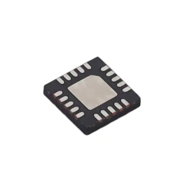
- Part No.:
- TCPP03-M20
- Manufacturer:
- STMicroelectronics
- Category:
- Surge Suppression Ics
- Package:
- 20-WFQFN Exposed Pad
- Datasheet:
-
 TCPP03-M20.pdf
- Description:
- USB-C POWER DELIVERY DUAL ROLE P
- Quantity:
- Payment:

- Shipping:

Inventory:1,507
Please send an inquiry. Send us your inquiry, and we will respond immediately.
Product details
Overview
TCPP03-M20 from STMicroelectronics is a USB-C Power Delivery 3.1 companion controller designed to interface with STM32 microcontrollers featuring integrated UCPD peripherals. It provides dual-role power (DRP) support up to 100 W (20 V/5 A SPR), embedded N-MOSFET gate drivers for consumer/provider paths, 24 V tolerance on VBUS and CC pins, and integrated VBUS/VCONN discharge. It enables cost-effective, MCU-based USB-C PD implementations in portable chargers and DRP-enabled docking stations.
For engineers reviewing the TCPP03-M20 datasheet, TCPP03-M20 pinout, TCPP03-M20 application, or TCPP03-M20 equivalent, this device is selected for its I²C-configurable OVP/OCP thresholds (1.16 V typical VOVP_TH on Vsense, 42 mV typical VTH_OCP_VBUS), dual-gate-driver architecture, dead-battery management, and USB-IF certified operation on X-NUCLEO-DRP1M1-G4 (TID6408).
Technical Context
The TCPP03-M20 operates as a hardware protection and signal conditioning companion to STM32 UCPD-capable MCUs - not a standalone PD controller. Its functional block integrates independent gate drivers (GDPg/GDCg), analog current sensing (Isense → IANA with 42 V/V gain), and configurable protection logic (OVP on VBUS at 1.16 V threshold, OCP at 42 mV across sense resistor), all managed via I²C with two selectable addresses (0x64/0x65).
It supports three I²C-controlled power modes: Hibernate (dead-battery enabled, FLGn indicates VBUS presence), Low Power (CC clamped at 5 V, no PD communication), and Normal (full performance, failure flagging via FLGn). VBUS turn-on time is 1–3 ms; OVP response is ≤145 ns; OCP reaction is 3–8 µs - enabling fast fault containment in bidirectional power paths.
Key Specifications
| Parameter | Value and Actual Design Meaning |
|---|---|
| VBUS OVP Threshold | 1.16 V on Vsense pin - sets 20 V OVP at 20:1 external resistor divider; enables precise, adjustable overvoltage cutoff before MCU damage |
| VBUS OCP Threshold | 42 mV across Rs - triggers shutdown at 5 A with 10 mΩ sense resistor; supports 100 W SPR compliance |
| VCONN OCP | 47 mA typical trip - protects 5 V VCONN supply against short circuits while maintaining USB-C spec-compliant 1 W delivery |
| I²C Address | 0x64 or 0x65 - LSB set by I2C_ADD pin (GND or 1.8/3.3 V); allows dual-device addressing on same bus without conflict |
| CC Pin ESD Rating | ±8 kV contact / ±15 kV air (IEC 61000-4-2 Level 4) - meets USB-C robustness requirements with external 100 nF CBIAS capacitor |
| Thermal Shutdown | 150 °C typical - disables gate drivers and asserts FLGn to prevent thermal runaway during sustained overload |
| VBUS Discharge Time | 220 ms - safely drains 20 V/100 µF bus capacitance via internal 2.5 kΩ path; eliminates residual voltage hazards |
Pinout & Package
TCPP03-M20 uses a QFN-20L package (4.0 × 4.0 × 0.75 mm) with exposed thermal pad (GND). The pinout supports full USB-C DRP functionality with separate gate drive, current/voltage sense, and dual CC channel routing.
| Pin/Terminal | Circuit Role | Design Meaning |
|---|---|---|
| CC1 / CC2 | UCPD interface (MCU side) | Low-voltage (≤5.5 V) differential signaling inputs/outputs connected directly to STM32 UCPD peripheral |
| CC1c / CC2c | USB-C connector interface | 24 V-tolerant CC pins with integrated 5.75 V OVP clamp and ESD protection; require external 100 nF CBIAS |
| GDPg / GDPs | Provider path gate driver | GDPg drives gate of external N-MOSFET; GDPs returns source node - enables low-Rds(on) sourcing with cost-effective N-FETs |
| GDCg / GDCs | Consumer path gate driver | GDCg drives sink-path N-MOSFET gate; GDCs returns source - supports bidirectional power with independent control |
| VSENSE / ISENSE | VBUS monitoring inputs | VSENSE measures VBUS voltage via resistor divider; ISENSE connects to shunt for analog current sensing (→ IANA output) |
| IANA | Analog current output | 42 V/V gain output (±2 mV offset) - delivers 1.95 V at OCP event; interfaces directly to MCU ADC without external op-amp |
| FLGn | Open-drain fault flag | Active-low indicator: VBUS presence in hibernate/low-power mode; OVP/OCP/OTP fault in normal mode (requires I²C register read) |
| EN / I2C_ADD | Power enable & address select | EN controls I²C voltage domain (1.8 V or 3.3 V); I2C_ADD sets LSB of 7-bit I²C address (0x64 or 0x65) |
Key Features
| Feature | Design Value |
|---|---|
| Dual independent N-MOSFET gate drivers | Enables use of low-cost, low-Rds(on) N-channel FETs instead of P-FETs - reduces BOM cost and board area vs ASIC-based PD solutions |
| Configurable VBUS OVP/OCP thresholds | I²C-adjustable trip points allow system-level tuning for different input sources (e.g., 15 V adapters, 20 V PPS) without hardware change |
| Integrated VBUS/VCONN discharge | On-chip 2.5 kΩ discharge paths eliminate need for external MOSFETs or RC networks - simplifies layout and improves safety certification |
| Dead-battery management | Automatic VBUS detection and wake-up in hibernate mode enables charging from 0 V battery - critical for portable devices with depleted cells |
| USB-IF certified operation | Validated on X-NUCLEO-DRP1M1-G4 (TID6408) - guarantees interoperability with certified chargers, cables, and accessories per USB PD 3.1 |
Applications
| USB-C Docking Station | Multi-Port Laptop Charger |
|---|---|
|
Use Scenario: A compact desktop dock providing simultaneous USB-C data, video, and up to 100 W power delivery to laptops. IC Role / Device Role / Timing Role: TCPP03-M20 acts as the hardware PD protection layer between the STM32 UCPD host and VBUS power path - managing gate drivers, OVP/OCP, and CC line robustness. Use Value: Enables single-chip MCU-based DRP implementation with <145 ns VBUS OVP response and ±15 kV CC ESD immunity - meeting USB-IF compliance without external protection ICs. |
Use Scenario: A GaN-based 65 W multi-port charger supporting simultaneous PD negotiation on two USB-C ports. IC Role / Device Role / Timing Role: TCPP03-M20 serves as the per-port PD companion, handling VBUS switching, current sensing (via IANA), and fault flagging for each output path. Use Value: Dual I²C addresses (0x64/0x65) allow independent configuration of both ports; integrated VCONN OCP (47 mA) ensures safe 5 V/1 W delivery to attached accessories. |
| Industrial Handheld Terminal | USB-C Powered Test Equipment |
|
Use Scenario: Ruggedized field terminal requiring hot-plug USB-C power input (5–20 V) and battery charging with dead-battery recovery. IC Role / Device Role / Timing Role: TCPP03-M20 manages VBUS UVLO (2.4 V), dead-battery wake-up, and bidirectional gate control - enabling reliable boot from 0 V battery. Use Value: Hibernate-mode FLGn indicates VBUS presence before MCU initialization; 24 V-tolerant CC pins withstand accidental 24 V misconnection during field use. |
Use Scenario: Benchtop oscilloscope or logic analyzer powered via USB-C with optional 20 V input for extended runtime. IC Role / Device Role / Timing Role: TCPP03-M20 provides VBUS OVP (adjustable via Vsense divider) and analog current monitoring (IANA) for real-time power telemetry and overload shutdown. Use Value: 42 V/V IANA gain and ±2 mV offset enable accurate 0–5 A measurement using standard 12-bit MCU ADC - eliminating external current-sense amplifier. |
Equivalent & Alternatives
The following parts are listed as comparable options for similar USB-C PD companion controller applications.
| Alternative Part | Technical Difference | Application Difference | Selection Advice |
|---|---|---|---|
| TI TUSB320LAIR | Standalone Type-C port controller with integrated PD PHY; no gate drivers; requires external FETs and discrete OVP/OCP | Targets simpler UFP/DFP-only designs; lacks DRP support and analog current sensing | Select when full PD protocol stack offload is needed and cost-per-FET is less critical than integration level |
| NXP PTN3364B | USB-C redriver/re-timer with limited PD awareness; no VBUS switching, OVP, or gate drivers | Designed for signal integrity enhancement only - not a PD protection or power path controller | Not functionally equivalent; avoid for power delivery control applications |
Compared with TUSB320LAIR and PTN3364B, the TCPP03-M20 uniquely combines MCU companion architecture, dual N-FET gate drivers, analog current sensing (IANA), and USB-IF certified DRP operation - delivering lower system BOM cost and faster fault response for STM32-based designs.
Availability
TCPP03-M20 is available at Aetrix Electronics and suitable for USB-C docking stations, multi-port GaN chargers, industrial handheld terminals, and USB-C-powered test equipment requiring stable component supply, long-term lifecycle support, and USB-IF compliance assurance.
Supply support for TCPP03-M20 includes scheduled delivery planning, volume procurement assistance, BOM continuity management, traceable sourcing, and lifecycle availability coordination for OEM customers, industrial embedded developers, connected-device designers, and electronics production programs.
Manufacturer
STMicroelectronics is a global semiconductor leader headquartered in Geneva, Switzerland, specializing in microcontrollers, analog ICs, power management, and automotive-grade components - with over 40 years of industrial reliability and broad ecosystem support.
The TCPP03-M20 belongs to ST's USB-C Power Delivery Companion portfolio, engineered specifically to extend STM32 UCPD capabilities with hardware-level protection, gate driving, and analog monitoring - enabling cost-optimized, certified PD implementations without dedicated PD ASICs.
FAQ
What is the purpose of the CBIAS pin?
The CBIAS pin connects to an external 100 nF, 50 V capacitor that forms part of the integrated ESD protection circuit for the CC1c and CC2c pins. This capacitor works with internal clamping diodes to absorb ±8 kV contact and ±15 kV air discharge events per IEC 61000-4-2 Level 4, ensuring robust USB-C connector-side immunity without additional TVS diodes.
How does the TCPP03-M20 support dead-battery operation?
In hibernate mode (ENABLE = low, VCC_VCONN = 0 V), the TCPP03-M20 monitors VBUS through internal UVLO (2.4 V typical) and asserts FLGn to indicate presence of input voltage - allowing the host MCU to wake up and initiate charging even when the system battery is fully depleted. No external biasing or auxiliary power is required.
Can the TCPP03-M20 be used without an STM32 UCPD MCU?
No - the TCPP03-M20 is explicitly designed as a companion device for STM32 MCUs with embedded UCPD peripherals. It lacks a built-in PD protocol engine and relies on the host MCU for PD message handling, policy engine execution, and state machine control via I²C. Standalone PD negotiation is not supported.
What is the maximum VBUS voltage the TCPP03-M20 can tolerate on its pins?
The TCPP03-M20 supports 24 V absolute maximum rating on VBUSc, CC1c, CC2c, GDPs, and GDCs pins per Table 2 of DS13618. This tolerance enables safe operation during transient overvoltage events - such as misconnected 24 V supplies or faulty chargers - while its internal OVP triggers at 20 V (configured via Vsense divider) to protect downstream circuitry.
TCPP03-M20 Specifications
- Product attributes
- Attribute value
- Manufacturer:
- STMicroelectronics
- Package/Case:
- 20-WFQFN Exposed Pad
- Series:
- -
- Packaging:
- Tape & Reel (TR)
- Product Status:
- Active
- Voltage - Clamping:
- 5V
- Technology:
- External Switch
- Number of Circuits:
- 1
- Applications:
- -
- Grade:
- -
- Qualification:
- -
- Mounting Type:
- Surface Mount
- Supplier Device Package:
- 20-QFN (4x4)
TCPP03-M20 FAQ
1.How can I place an order for TCPP03-M20 through Aetrix?
Please submit a Request for Quotation (RFQ) for TCPP03-M20 on Aetrix. Our sales agent will provide a competitive quotation and guide you through the order confirmation once you accept the terms.
2.Are the price and stock information for TCPP03-M20 reliable?
The price and inventory of TCPP03-M20 are updated periodically and may fluctuate due to market conditions. Stock and pricing data are typically refreshed every 24 hours. Quotation validity for TCPP03-M20 is usually 5 days.
3.What payment methods are accepted for TCPP03-M20?
We accept Wire Transfer, PayPal, Credit Card, Western Union, MoneyGram, and Escrow for TCPP03-M20 transactions.
Note: Certain payment methods may incur a processing fee.
4.How is shipping managed for TCPP03-M20?
TCPP03-M20 orders can be shipped via leading logistics carriers, including DHL, UPS, FedEx, TNT, or Registered Mail.
Once your TCPP03-M20 order is processed, you will receive an email with the shipment details and tracking number.
Note: Tracking information may take up to 24 hours to appear. Express delivery typically takes 3–5 business days.
5.How can I obtain technical support or documentation for TCPP03-M20?
For technical support, including TCPP03-M20 datasheets, pinout diagrams, or application guidance, please contact our engineering support team. They can provide detailed documentation and assistance for your TCPP03-M20 requirements.
6.How does Aetrix verify that TCPP03-M20 is sourced from the original manufacturer or authorized distributors?
All TCPP03-M20 products on Aetrix are procured from qualified distributors and authorized channels. Our dedicated quality assurance team conducts strict verification, including traceability checks and, if necessary, third-party testing. This ensures that TCPP03-M20 meets industry standards.
7.What is the process for return or replacement of TCPP03-M20?
All TCPP03-M20 units undergo pre-shipment inspection (PSI). If there is an issue with TCPP03-M20, returns or replacements are accepted under the following conditions:
1.Quantity discrepancies, incorrect items, or visible external defects (such as breakage or corrosion), acknowledged by Aetrix.
2.The issue is reported within 90 days of delivery.
3.The TCPP03-M20 part is unused and in its original packaging.
Return procedure for TCPP03-M20:
1.Submit a request within 90 days.
2.Obtain a Return Material Authorization (RMA) from Aetrix.
TCPP03-M20 Tags
-
TVS3300DRVR
Texas Instruments

-
TCPP01-M12
STMicroelectronics
-
TPD4S214YFFR
Texas Instruments
-
TPD6S300ARUKR
Texas Instruments
-
TBU-CA085-300-WH
Bourns Inc.
-
TBU-CA065-500-WH
Bourns Inc.
-
TBU-CA040-100-WH
Bourns Inc.
-
TBU-CA085-500-WH
Bourns Inc.
-
TBU-CA085-200-WH
Bourns Inc.
-
NX20P0408UKZ
NXP Semiconductors
-
TBU-CA085-100-WH
Bourns Inc.
-
TBU-CA050-300-WH
Bourns Inc.
Tech Hub

A practical engineering guide to 3.3V and 5V logic compatibility, input thresholds, resistor dividers, translator ICs, MOSFET level shifting, I2C pull-ups, timing limits and power-sequencing risks.

The 74HC595 uses push-pull logic outputs, while the TPIC6B595 uses 50 V open-drain DMOS sinks for higher-power loads. This guide compares timing, current limits, 3.3 V interfacing, load wiring, thermal…

The 74HC595 converts serial data into eight stable parallel outputs. This guide covers pin functions, shift and storage timing, OE and MR behavior, drive-current limits, cascading, voltage compatibilit…

A technical comparison of level-sensitive latches and edge-triggered flip-flops, covering timing windows, setup and hold limits, master–slave operation, time borrowing, race-through, HDL inference and…

A D latch stores one bit while Enable controls when data can pass. This reference covers gate-level operation, truth tables, transparency, setup and hold timing, LE versus OE, common ICs and practical …

An SR latch stores one bit through cross-coupled feedback. This engineering reference covers NOR and NAND implementations, truth tables, forbidden-state recovery, gated operation, switch debouncing, fa…

Latch circuits retain one bit through feedback. This technical reference covers SR and D latches, truth tables, transparency, timing limits, latch-versus-flip-flop behavior, applications and common log…

An engineering guide to LED driver operation, constant-current and constant-voltage outputs, linear and switching topologies, dimming, IC selection, calculations, replacement compatibility, and fault c…

Operational amplifier guide covering op amp basics, feedback, ideal vs real op amps, common configurations, buffer circuits, offset, bias current, gain-bandwidth, slew rate, rail-to-rail limits and sel…

Jumper cables guide covering safe connection order, red and black clamp placement, final ground connection, cable gauge, length, clamp quality, copper vs CCA cables, jump starter comparison and battery…


