
 My Inquiry
 My Account


STMicroelectronics TDA7293HS
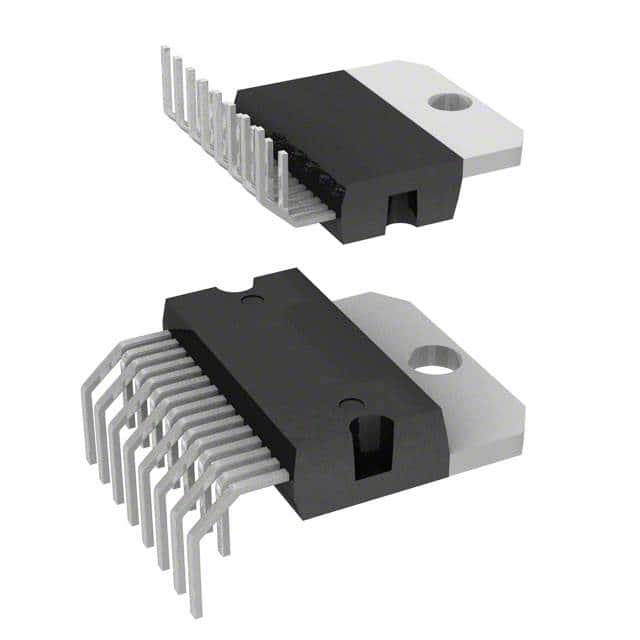
- Part No.:
- TDA7293HS
- Manufacturer:
- STMicroelectronics
- Category:
- Audio Amplifiers
- Package:
- Multiwatt-15 (Horizontal, Bent and Staggered Leads)
- Datasheet:
-
 TDA7293HS.pdf
- Description:
- IC AMP AB MONO 100W 15MULTIWATT
- Quantity:
- Payment:

- Shipping:

Inventory:3,817
Please send an inquiry. Send us your inquiry, and we will respond immediately.
Product details
Overview
TDA7293HS from STMicroelectronics is a monolithic Class AB audio power amplifier in Multiwatt15H package, designed for high-fidelity applications including home stereo, self-powered loudspeakers, and premium TV audio systems. It delivers 100 W into 8 Ω at ±40 V supply with ≤0.1% THD (20 Hz–15 kHz), features integrated mute/standby control, thermal shutdown at 160 °C, and DMOS output stage enabling ±50 V operating voltage range.
For engineers reviewing the TDA7293HS datasheet, TDA7293HS pinout, TDA7293HS application, or TDA7293HS equivalent, key selection considerations include its dual power rail architecture (+Vs/-Vs signal + +PWVs/-PWVs power), clip detection on Pin 5, bootstrap loader capability (Pin 12), and modular parallel operation support via Pin 11 - all critical for low-impedance, high-power audio system design.
Technical Context
The TDA7293HS implements a DMOS-based unity-gain output buffer with local linearizing feedback to minimize crossover distortion while maintaining stable quiescent current across temperature. Its BCDII 100/120 mixed bipolar-MOS process eliminates second breakdown, enabling safe operation into reactive 4 Ω loads at ±50 V supply.
Protection integrates dynamic SOA limiting with localized thermal sensing: device mutes at 150 °C junction temperature and enters standby at 160 °C. Standby and mute functions are CMOS-compatible, independently controlled, and sequenced to eliminate switch-on/off pop noise - verified by recommended turn-on/off timing in Figure 5 of the datasheet.
Key Specifications
| Parameter | Value and Actual Design Meaning |
|---|---|
| Output Power | 100 W into 8 Ω @ THD = 10%, VS = ±40 V - enables full-range high-SPL audio reproduction without external paralleling |
| Supply Voltage Range | ±12 V to ±50 V - supports wide-range DC supplies and high-voltage rail designs up to 100 V peak differential |
| Total Harmonic Distortion | ≤0.1% (20 Hz–15 kHz, 0.1–50 W) - meets Hi-Fi linearity requirements for critical listening environments |
| Thermal Shutdown Threshold | 160 °C junction - triggers hard standby after muting at 150 °C, preventing latch-up during sustained overload |
| Input Offset Voltage | ±10 mV - ensures minimal DC offset at output, reducing coupling capacitor size and low-frequency phase shift |
| Open-Loop Gain | 80 dB - provides sufficient loop gain for stable closed-loop operation with 30 dB (1000×) configured gain |
| Quiescent Current | 50–100 mA - balances idle power dissipation against output stage bias stability across temperature |
| Clip Detection Output | Duty-cycle-modulated signal on Pin 5 - enables real-time clipping monitoring without external comparators or ADCs |
Pinout & Package
The TDA7293HS uses the horizontally mounted Multiwatt15H package (15-pin, tab-connected to Pin 8), optimized for surface-mount heatsink attachment and high-power thermal management in compact audio chassis layouts.
| Pin/Terminal | Circuit Role | Design Meaning |
|---|---|---|
| 1 | STBY-GND | Standby reference node tied to -Vs; sets logic threshold for standby activation (3.5 V min to exit) |
| 2 | IN− | Inverting input; accepts differential or single-ended signals with 100 kΩ input resistance |
| 3 | IN+ | Non-inverting input; used with R1/R3 for gain setting (default 30 dB via 22 kΩ resistors) |
| 4 | MUTE | CMOS-compatible mute control; <1.5 V mutes, >3.5 V unmutes - suppresses output before power-up transients |
| 5 | CLIP DET | Open-collector clip indicator; outputs duty-cycle-modulated signal proportional to clipping duration |
| 6 | BOOTSTRAP | Bootstrap capacitor connection point; supports dual configuration (to Pin 14 or Pin 12) for 100 V or 120 V max swing |
| 7 | SGND | Signal ground reference; isolated from power ground to reduce noise coupling in split-rail designs |
| 8 | TAB / −Vs (Signal) | Exposed metal tab electrically connected to Pin 8; must be thermally bonded to heatsink and tied to signal −Vs rail |
| 9 | VSTBY | Standby control input; referenced to −Vs (Pin 8); activates standby mode when pulled >3.5 V |
| 10 | VMUTE | Mute control input; referenced to −Vs (Pin 8); activates mute when pulled >3.5 V |
| 11 | BUFFER DRIVER | Modular master/slave interface; enables parallel operation by driving slave devices' input stages |
| 12 | BOOT LOADER | Clamped bootstrap reference; tracks output up to 100 V then clamps - extends safe output swing to VS − 3 V |
| 13 | −PWVs | Negative power supply for output stage; isolated from signal −Vs to reduce power-stage noise injection |
| 14 | OUT | Amplified output; capable of ±6.5 A peak current into 4 Ω - requires external Boucherot network if long speaker cables used |
| 15 | +PWVs | Positive power supply for output stage; isolated from signal +Vs to maintain PSRR >75 dB at 100 Hz |
Key Features
| Feature | Design Value |
|---|---|
| Dual isolated power rails | +Vs/−Vs (signal path) and +PWVs/−PWVs (output stage) - improves PSRR by >15 dB and reduces intermodulation distortion |
| Bootstrap loader (Pin 12) | Clamps at 100 V while tracking output - enables full 120 V technology voltage swing without external clamp diodes |
| Modular parallel operation | Pins 4, 9, 11, and SGND enable master/slave configuration for >200 W into 2 Ω - no ballast resistors required between outputs |
| Pop-noise suppression | Sequenced mute-before-standby and standby-before-mute transitions - eliminates audible transients during power cycling |
| Integrated clip detection | Active-duty output on Pin 5 - allows LED indicators or microcontroller-triggered gain reduction without analog-to-digital conversion |
| Thermal foldback protection | Mutes at 150 °C, shuts down at 160 °C - preserves device integrity during sustained overload without requiring external thermal sensors |
Applications
| Home Stereo Amplifiers | Self-Powered Loudspeakers |
|---|---|
Use Scenario: Dual-channel 100 W/channel amplifier in compact bookshelf or floor-standing speaker enclosures with integrated DSP and digital inputs. IC Role / Device Role / Timing Role: Final power stage delivering high-current, low-distortion analog output to voice coils; operates in Class AB with adjustable bias via external R5/C3 network. Use Value: Delivers 100 W into 8 Ω with ≤0.005% THD at 1 W - preserves transient fidelity and dynamic range expected in audiophile-grade playback. | Use Scenario: Active subwoofer module with built-in crossover, EQ, and RMS compression, housed in sealed or ported cabinet. IC Role / Device Role / Timing Role: High-current low-frequency driver; handles 20–200 Hz band with high damping factor (>200) due to low output impedance (<0.1 Ω). Use Value: Sustains 90 W continuous into 4 Ω at 40 Hz - enables deep bass extension without thermal throttling or protection-induced dropouts. |
| Premium TV Audio Systems | Hi-Fi Bridge-Mode Subwoofers |
Use Scenario: Integrated soundbar or rear-channel amplifier in 5.1/7.1 TV audio platforms requiring ultra-low EMI and compact thermal footprint. IC Role / Device Role / Timing Role: Mid/high-frequency channel amplifier; powered from shared ±35 V rails with fast transient response (5 V/µs slew rate). Use Value: Achieves 75 W into 8 Ω with <10 µV input-referred noise - prevents hiss in quiet program material and maintains SNR >105 dB(A). | Use Scenario: Dual-TDA7293 bridge-tied load (BTL) configuration driving 8–16 Ω subwoofer loads in studio monitors or high-end AV receivers. IC Role / Device Role / Timing Role: Master-slave BTL pair; one device inverted, both synchronized via shared mute/standby and bootstrap lines. Use Value: Delivers 200 W into 16 Ω at ±40 V - doubles voltage swing while halving current demand per device, improving thermal margin by 40%. |
Equivalent & Alternatives
The following parts are listed as comparable options for similar high-voltage audio amplifier applications.
| Alternative Part | Technical Difference | Application Difference | Selection Advice |
|---|---|---|---|
| TDA7294V | Same Multiwatt15V package; lower max supply (±40 V vs ±50 V); no bootstrap loader (Pin 12); 70 W into 8 Ω | Limited to 140 W peak in BTL; unsuitable for >100 V rail designs or modular configurations requiring Pin 12 clamping | Select TDA7294V only for cost-sensitive, lower-power designs where 120 V swing and modular scaling are not required. |
| LM3886TF | TO-264 package; ±42 V max; no mute/standby pins; no clip detection; 68 W into 8 Ω; no dual power rails | Requires external mute circuitry and thermal monitoring; lacks integrated protection sequencing and modular interface | Choose LM3886TF for discrete-style designs needing proven reliability but accepting higher board area and added component count. |
Compared with TDA7294V and LM3886TF, the TDA7293HS uniquely combines 120 V technology headroom, integrated clip detection, and modular master/slave capability - making it the only option supporting scalable, pop-free, high-efficiency audio systems above 100 W without external support ICs.
Availability
TDA7293HS is available at Aetrix Electronics and suitable for home stereo amplifiers, self-powered loudspeakers, and premium TV audio systems requiring stable component supply, long-lifecycle assurance, and consistent thermal performance across production batches.
Supply support for TDA7293HS includes scheduled delivery planning, volume procurement assistance, BOM continuity management, traceable sourcing, and lifecycle availability coordination for OEM customers, industrial embedded developers, connected-device designers, and electronics production programs.
Manufacturer
STMicroelectronics is a global semiconductor leader headquartered in Geneva, Switzerland, specializing in analog, power, and automotive ICs with over 45 years of high-reliability product development.
The TDA7293HS belongs to ST's high-voltage audio amplifier product line, engineered specifically for Hi-Fi and professional audio applications demanding >100 W output, ultra-low distortion, and robust protection in compact form factors.
FAQ
What is the maximum safe supply voltage for TDA7293HS with bootstrap connected between Pins 6 and 12?
The TDA7293HS supports up to ±60 V supply (120 V differential) when the bootstrap capacitor is connected between Pin 6 (BOOTSTRAP) and Pin 12 (BOOT LOADER), thanks to the internal 100 V clamp on Pin 12 that prevents overvoltage stress on the bootstrap node during high-swing operation.
How does the modular parallel operation work, and what pins must be connected between master and slave devices?
In modular mode, the master device drives slaves via Pin 11 (BUFFER DRIVER); slave IN+ and IN− are tied to −Vs, SGND is connected to −Vs, and STBY/MUTE pins are ganged. Outputs connect directly without ballast resistors, and bootstrap capacitors scale linearly (22 µF × N devices) per the datasheet's Figure 11.
Can TDA7293HS be used in bridge-tied load (BTL) configuration, and what are the minimum load requirements?
Yes - two TDA7293HS devices can be configured in BTL mode with one inverted. The minimum safe load is 8 Ω to limit peak current and thermal dissipation; at ±25 V supply, this yields 150 W output, and at ±40 V into 16 Ω, it delivers 200 W while maintaining SOA compliance per Section 4.3 of the datasheet.
What is the function of Pin 5 (CLIP DET), and how is it typically interfaced in a production design?
Pin 5 outputs an open-collector duty-cycle signal proportional to clipping duration - e.g., 40% duty cycle at 10% THD. In production, it's typically pulled up to 5 V via 10 kΩ and fed to an MCU GPIO for real-time gain adjustment or to drive an LED via a transistor for visual overload indication without analog signal processing.
TDA7293HS Specifications
- Product attributes
- Attribute value
- Manufacturer:
- STMicroelectronics
- Series:
- -
- Package/Case:
- Multiwatt-15 (Horizontal, Bent and Staggered Leads)
- Packaging:
- Tube
- Product Status:
- Obsolete
- Type:
- Class AB
- Output Type:
- 1-Channel (Mono)
- Max Output Power x Channels @ Load:
- 100W x 1 @ 4Ohm
- Voltage - Supply:
- ±12V ~ 50V
- Features:
- Depop, Differential Inputs, Mute, Short-Circuit and Thermal Protection, Standby
- Mounting Type:
- Through Hole
- Operating Temperature:
- 0°C ~ 70°C (TA)
- Grade:
- -
- Qualification:
- -
- Supplier Device Package:
- 15-Multiwatt
TDA7293HS FAQ
1.How can I place an order for TDA7293HS through Aetrix?
Please submit a Request for Quotation (RFQ) for TDA7293HS on Aetrix. Our sales agent will provide a competitive quotation and guide you through the order confirmation once you accept the terms.
2.Are the price and stock information for TDA7293HS reliable?
The price and inventory of TDA7293HS are updated periodically and may fluctuate due to market conditions. Stock and pricing data are typically refreshed every 24 hours. Quotation validity for TDA7293HS is usually 5 days.
3.What payment methods are accepted for TDA7293HS?
We accept Wire Transfer, PayPal, Credit Card, Western Union, MoneyGram, and Escrow for TDA7293HS transactions.
Note: Certain payment methods may incur a processing fee.
4.How is shipping managed for TDA7293HS?
TDA7293HS orders can be shipped via leading logistics carriers, including DHL, UPS, FedEx, TNT, or Registered Mail.
Once your TDA7293HS order is processed, you will receive an email with the shipment details and tracking number.
Note: Tracking information may take up to 24 hours to appear. Express delivery typically takes 3–5 business days.
5.How can I obtain technical support or documentation for TDA7293HS?
For technical support, including TDA7293HS datasheets, pinout diagrams, or application guidance, please contact our engineering support team. They can provide detailed documentation and assistance for your TDA7293HS requirements.
6.How does Aetrix verify that TDA7293HS is sourced from the original manufacturer or authorized distributors?
All TDA7293HS products on Aetrix are procured from qualified distributors and authorized channels. Our dedicated quality assurance team conducts strict verification, including traceability checks and, if necessary, third-party testing. This ensures that TDA7293HS meets industry standards.
7.What is the process for return or replacement of TDA7293HS?
All TDA7293HS units undergo pre-shipment inspection (PSI). If there is an issue with TDA7293HS, returns or replacements are accepted under the following conditions:
1.Quantity discrepancies, incorrect items, or visible external defects (such as breakage or corrosion), acknowledged by Aetrix.
2.The issue is reported within 90 days of delivery.
3.The TDA7293HS part is unused and in its original packaging.
Return procedure for TDA7293HS:
1.Submit a request within 90 days.
2.Obtain a Return Material Authorization (RMA) from Aetrix.
TDA7293HS Tags
-Exposed-Pad.jpg)
-
TS34119CS RLG
Taiwan Semiconductor Corporation

-
LM386MX-1/NOPB
Texas Instruments

-
TPA711DGNR
Texas Instruments

-
LM386N-4/NOPB
Texas Instruments

-
TS4990IST
STMicroelectronics
-
PAM8302AASCR
Diodes Incorporated
-
TPA6130A2RTJR
Texas Instruments
-
TPA6111A2DGNR
Texas Instruments
-
LM4861MX/NOPB
Texas Instruments
-
LM386M-1/NOPB
Texas Instruments

-
NCS2211DR2G
onsemi
-
IS31AP2005-DLS2-TR
Lumissil Microsystems
Tech Hub

A practical engineering and sourcing framework covering lifecycle verification, lifetime-buy calculations, replacement qualification, supplier checks and counterfeit-risk controls.

TTL and CMOS logic families differ in thresholds, loading, output drive, power and timing. This engineering guide compares 74HC and 74HCT, calculates noise margins and checks 3.3 V/5 V compatibility.

A practical engineering guide to 3.3V and 5V logic compatibility, input thresholds, resistor dividers, translator ICs, MOSFET level shifting, I2C pull-ups, timing limits and power-sequencing risks.

The 74HC595 uses push-pull logic outputs, while the TPIC6B595 uses 50 V open-drain DMOS sinks for higher-power loads. This guide compares timing, current limits, 3.3 V interfacing, load wiring, thermal…

The 74HC595 converts serial data into eight stable parallel outputs. This guide covers pin functions, shift and storage timing, OE and MR behavior, drive-current limits, cascading, voltage compatibilit…

A technical comparison of level-sensitive latches and edge-triggered flip-flops, covering timing windows, setup and hold limits, master–slave operation, time borrowing, race-through, HDL inference and…

A D latch stores one bit while Enable controls when data can pass. This reference covers gate-level operation, truth tables, transparency, setup and hold timing, LE versus OE, common ICs and practical …

An SR latch stores one bit through cross-coupled feedback. This engineering reference covers NOR and NAND implementations, truth tables, forbidden-state recovery, gated operation, switch debouncing, fa…

Latch circuits retain one bit through feedback. This technical reference covers SR and D latches, truth tables, transparency, timing limits, latch-versus-flip-flop behavior, applications and common log…

An engineering guide to LED driver operation, constant-current and constant-voltage outputs, linear and switching topologies, dimming, IC selection, calculations, replacement compatibility, and fault c…


