
 My Inquiry
 My Account


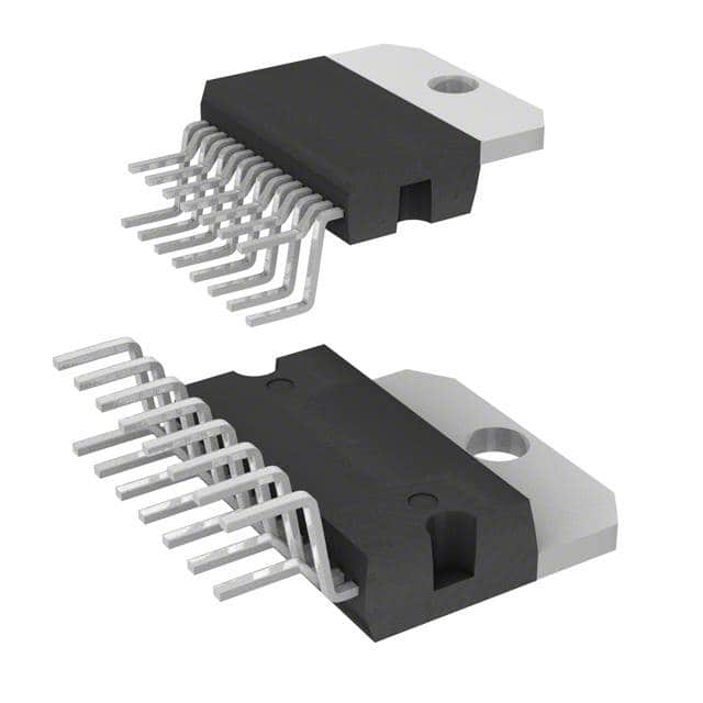
STMicroelectronics TDA7293V
- Part No.:
- TDA7293V
- Manufacturer:
- STMicroelectronics
- Category:
- Audio Amplifiers
- Package:
- Multiwatt-15 (Vertical, Bent and Staggered Leads)
- Datasheet:
-
 TDA7293V.pdf
- Description:
- IC AMP AB MONO 100W 15MULTIWATT
- Quantity:
- Payment:

- Shipping:

Inventory:770
Please send an inquiry. Send us your inquiry, and we will respond immediately.
Product details
Overview
TDA7293V from STMicroelectronics is a monolithic Class AB audio power amplifier IC in Multiwatt15V package, designed for high-fidelity audio output stages. It delivers 100 W into 8 Ω at ±40 V supply with 10% THD, features integrated mute and standby functions with CMOS-compatible control inputs, and supports modular parallel operation for low-impedance loads in home stereo and powered loudspeaker systems.
For engineers reviewing the TDA7293V datasheet, TDA7293V pinout, TDA7293V application, or TDA7293V equivalent, key selection considerations include its ±50 V operating voltage range, DMOS output stage, thermal shutdown at 160 °C, clip detection on Pin 5, and bootstrap-capable dual power supply architecture (±Vs signal + ±PWVs power rails).
Technical Context
The TDA7293V employs Multipower BCD II 100/120 technology to combine bipolar precision circuitry with DMOS power transistors, eliminating second breakdown limitations and enabling safe operation into reactive 4 Ω and 8 Ω loads. Its output stage uses local linearizing feedback and Miller compensation to maintain low distortion across frequency.
Protection includes dynamic SOA limiting via local temperature sensing, thermal shutdown (mute at 150 °C, standby at 160 °C), short-circuit protection with no input signal applied, and ESD tolerance of ±1500 V HBM. Mute and standby are independently controlled via logic-level pins with defined thresholds (1.5 V ON / 3.5 V OFF) and attenuation >70 dB.
Key Specifications
| Parameter | Value and Actual Design Meaning |
|---|---|
| Supply Voltage Range | ±12 V to ±50 V - Enables high-power delivery into 4 Ω/8 Ω loads without external boost converters. |
| Output Power | 100 W into 8 Ω @ THD = 10%, VS = ±40 V - Meets Hi-Fi amplifier requirements for self-powered speakers and premium TV audio. |
| Total Harmonic Distortion | 0.005 % typ. @ 5 W, 1 kHz - Ensures audibly transparent signal reproduction in critical listening environments. |
| Thermal Resistance (Junction-to-Case) | 1.0 °C/W typ. - Requires heatsink thermal resistance ≤ 2.2 °C/W for continuous 20 W average output in high-efficiency mode. |
| Standby Attenuation | 70–90 dB - Suppresses residual noise during system idle, critical for always-on smart speaker designs. |
| Mute Threshold Voltage | 1.5 V (ON), 3.5 V (OFF) referenced to –VS - Compatible with standard 3.3 V/5 V microcontroller GPIO without level-shifting. |
| Clip Detection Output | Duty-cycle-modulated signal on Pin 5 - Provides real-time overdrive monitoring for DSP-based loudness control or protection logic. |
Pinout & Package
The TDA7293V is housed in a vertically mounted Multiwatt15V package with exposed metal tab (Pin 8) thermally and electrically connected to –VS (power ground). The 15-pin layout supports dual-rail power separation (signal and power supplies), bootstrap operation, and modular parallel configuration via Pin 11.
| Pin/Terminal | Circuit Role | Design Meaning |
|---|---|---|
| 1 | STBY-GND | Standby function reference node; tied to –VS for proper threshold referencing and thermal path continuity. |
| 2 | IN– | Inverting input; accepts differential or single-ended signals with 100 kΩ input resistance and <10 mV offset. |
| 3 | IN+ | Non-inverting input; used with IN– for balanced operation or as single-ended input with R1/R3 bias network. |
| 4 | MUTE | CMOS-compatible mute control input; active-low logic with 1.5 V turn-on threshold referenced to –VS. |
| 5 | CLIP DET | Open-collector output indicating clipping; duty cycle scales with output overdrive magnitude (10–50 %). |
| 6 | BOOTSTRAP | Bootstrap capacitor connection point; enables rail-boosted gate drive for extended output swing up to ±120 V. |
| 7 | SGND | Signal ground; isolated from power ground to minimize noise coupling between analog and power sections. |
| 8 | –VS (Power) | Power supply return; tab-connected for low-inductance thermal path and high-current return routing. |
| 9 | VSTBY | Standby control input; CMOS-compatible with 1.5 V ON / 3.5 V OFF thresholds and <1 mA quiescent current in standby. |
| 10 | VMUTE | Mute control input; independent of standby, enabling silent power-up sequences and DSP-controlled muting. |
| 11 | MODULAR | Parallel-mode enable; connects master/slave devices for synchronized output stage operation without ballast resistors. |
| 12 | BOOT LOADER | Clamped bootstrap reference; limits voltage to 100 V, enabling full 120 V technology rating when bootstrapping to Pin 6. |
| 13 | –PWVs | Negative power supply rail for output stage; separate from signal –VS to reduce PSRR degradation at high output currents. |
| 14 | OUT | Amplified output; capable of ±6.5 A peak current into reactive loads with integrated short-circuit protection. |
| 15 | +PWVs | Positive power supply rail for output stage; decoupled separately from signal +Vs to maintain stability under dynamic load conditions. |
Key Features
| Feature | Design Value |
|---|---|
| DMOS Power Stage | Eliminates second breakdown risk, enabling robust operation into 4 Ω loads at ±50 V without SOA derating. |
| Dual-Rail Power Architecture | Separate ±Vs (signal) and ±PWVs (power) supplies reduce supply-induced distortion and improve PSRR by >75 dB. |
| Integrated Clip Detector | Provides duty-cycle modulated output on Pin 5 for real-time overdrive monitoring without external comparators. |
| Modular Parallel Operation | Pin 11 enables seamless connection of multiple TDA7293V units to drive sub-2 Ω loads while maintaining thermal balance. |
| Bootstrap-Enhanced Output Swing | Supports up to ±120 V rail operation via Pin 6/Pin 12 connection, extending peak power capability beyond standard ±100 V limits. |
Applications
| Home Stereo Amplifiers | Self-Powered Loudspeakers |
|---|---|
Use Scenario: High-fidelity two-channel amplification in compact floor-standing or bookshelf speakers with built-in DSP and Bluetooth streaming. IC Role / Device Role / Timing Role: Final output stage delivering 100 W/channel into 8 Ω with <0.01 % THD, using mute/stby for seamless source switching and thermal management. Use Value: Eliminates need for discrete MOSFET output stages while meeting EN55032 conducted emissions limits due to integrated EMI-reducing bootstrap architecture. | Use Scenario: Active bass module in 2.1 or 5.1 multimedia speaker systems requiring high-current, low-distortion low-frequency drive. IC Role / Device Role / Timing Role: Dedicated subwoofer amplifier with clip detection feeding DSP limiter algorithms, leveraging modular mode to parallel two units for 200 W into 4 Ω. Use Value: Achieves 150 W RMS output at 40 Hz with <0.05 % THD-enabling deep-bass extension without audible compression artifacts. |
| Top-Class Flat-Panel TV Audio | Hi-Fi Bridge-Mode Subwoofers |
Use Scenario: Integrated audio engine in premium 4K/8K TVs where space-constrained chassis demand high power density and low heat generation. IC Role / Device Role / Timing Role: Dual-mono channel amplifier with independent mute/stby control per channel, synchronized to HDMI CEC power commands. Use Value: Delivers 80 W/channel at 1 % THD into 8 Ω while maintaining <1 µV input-referred noise-preserving dialog clarity in cinematic content. | Use Scenario: High-power subwoofer driver in audiophile-grade home theater systems using bridge-tied load (BTL) configuration. IC Role / Device Role / Timing Role: One TDA7293V per side in BTL mode, with matched gain-setting resistors and shared bootstrap networks for phase coherence. Use Value: Generates 150 W into 8 Ω at ±25 V supply-reducing power supply size/cost versus single-ended 100 W designs while maintaining <0.1 % THD up to 100 Hz. |
Equivalent & Alternatives
The following parts are listed as comparable options for similar high-voltage audio amplifier applications.
| Alternative Part | Technical Difference | Application Difference | Selection Advice |
|---|---|---|---|
| TDA7294V | Lower max supply (±40 V vs ±50 V); 70 W into 8 Ω; no clip detector; same Multiwatt15V package. | Suitable for cost-sensitive mid-tier audio where 100 W headroom and real-time clipping feedback are not required. | Select TDA7294V only if system supply is capped at ±40 V and thermal budget allows higher dissipation per watt. |
| LM3886TF | Bipolar output stage; ±35 V max supply; 68 W into 8 Ω; no mute/stby; TO-220 package; no modular capability. | Fits legacy PCB layouts with TO-220 footprints; lacks integrated protection logic and multi-device synchronization. | Choose LM3886TF only when retrofitting existing designs or when discrete thermal sensor integration is preferred over monolithic shutdown. |
Compared with TDA7294V and LM3886TF, the TDA7293V uniquely combines ±50 V operation, clip detection, mute/stby logic, and modular parallel support-making it the sole option for scalable, feature-rich, high-power monolithic audio systems requiring design longevity and serviceability.
Availability
TDA7293V is available at Aetrix Electronics and suitable for home stereo amplifiers, self-powered loudspeakers, and top-class flat-panel TV audio systems requiring stable component supply, long-term lifecycle support, and traceable sourcing.
Supply support for TDA7293V includes scheduled delivery planning, volume procurement assistance, BOM continuity management, traceable sourcing, and lifecycle availability coordination for OEM customers, industrial embedded developers, connected-device designers, and electronics production programs.
Manufacturer
STMicroelectronics is a global semiconductor leader headquartered in Geneva, Switzerland, specializing in analog, power, and automotive ICs with vertical manufacturing capabilities and AEC-Q100 qualified processes.
The TDA7293V belongs to ST's high-voltage audio amplifier product line, engineered specifically for Hi-Fi and professional audio applications demanding >100 W output, ultra-low distortion, and integrated system-level features like mute, standby, and thermal protection.
FAQ
What is the maximum safe supply voltage for TDA7293V with bootstrap connected between Pins 6 and 12?
The absolute maximum supply voltage is ±60 V with no signal applied, but continuous operation with signal is rated to ±50 V. When bootstrap is connected between Pin 6 and Pin 12, the internal clamp at Pin 12 enables full 120 V technology rating-allowing ±50 V rails with 20 V headroom for transient peaks without capacitor overvoltage.
How does the modular parallel mode affect thermal management compared to single-device operation?
In modular mode, total output current capacity scales linearly with device count, but thermal dissipation per device decreases due to current sharing. For N devices, the bootstrap capacitor must be increased to 22 µF × N, and all SGND pins must connect to –VS to maintain consistent thermal reference-ensuring junction temperatures remain balanced within ±2 °C across units.
Can TDA7293V be used in bridge-tied load (BTL) configuration, and what are the minimum load requirements?
Yes, TDA7293V supports BTL operation using two devices per channel. Minimum load is 8 Ω to prevent excessive current stress on the DMOS output stage; at ±25 V supply, this yields 150 W output. Using lower impedances risks exceeding the 6.5 A current limit and triggering short-circuit protection during transients.
What is the functional difference between Pin 7 (SGND) and Pin 8 (–VS), and why must they be kept separate?
Pin 7 (SGND) is the low-noise analog reference for input and feedback circuitry, while Pin 8 (–VS) is the high-current power return for the DMOS output stage. Separating them prevents large-signal switching noise from modulating the input stage-measured PSRR improves by >20 dB at 1 kHz when SGND is routed directly to input decoupling capacitors instead of joining –VS at the bulk capacitor.
TDA7293V Specifications
- Product attributes
- Attribute value
- Manufacturer:
- STMicroelectronics
- Series:
- -
- Package/Case:
- Multiwatt-15 (Vertical, Bent and Staggered Leads)
- Packaging:
- Tube
- Product Status:
- Active
- Type:
- Class AB
- Output Type:
- 1-Channel (Mono)
- Max Output Power x Channels @ Load:
- 100W x 1 @ 4Ohm
- Voltage - Supply:
- ±12V ~ 50V
- Features:
- Depop, Differential Inputs, Mute, Short-Circuit and Thermal Protection, Standby
- Mounting Type:
- Through Hole
- Operating Temperature:
- 0°C ~ 70°C (TA)
- Grade:
- -
- Qualification:
- -
- Supplier Device Package:
- 15-Multiwatt
TDA7293V FAQ
1.How can I place an order for TDA7293V through Aetrix?
Please submit a Request for Quotation (RFQ) for TDA7293V on Aetrix. Our sales agent will provide a competitive quotation and guide you through the order confirmation once you accept the terms.
2.Are the price and stock information for TDA7293V reliable?
The price and inventory of TDA7293V are updated periodically and may fluctuate due to market conditions. Stock and pricing data are typically refreshed every 24 hours. Quotation validity for TDA7293V is usually 5 days.
3.What payment methods are accepted for TDA7293V?
We accept Wire Transfer, PayPal, Credit Card, Western Union, MoneyGram, and Escrow for TDA7293V transactions.
Note: Certain payment methods may incur a processing fee.
4.How is shipping managed for TDA7293V?
TDA7293V orders can be shipped via leading logistics carriers, including DHL, UPS, FedEx, TNT, or Registered Mail.
Once your TDA7293V order is processed, you will receive an email with the shipment details and tracking number.
Note: Tracking information may take up to 24 hours to appear. Express delivery typically takes 3–5 business days.
5.How can I obtain technical support or documentation for TDA7293V?
For technical support, including TDA7293V datasheets, pinout diagrams, or application guidance, please contact our engineering support team. They can provide detailed documentation and assistance for your TDA7293V requirements.
6.How does Aetrix verify that TDA7293V is sourced from the original manufacturer or authorized distributors?
All TDA7293V products on Aetrix are procured from qualified distributors and authorized channels. Our dedicated quality assurance team conducts strict verification, including traceability checks and, if necessary, third-party testing. This ensures that TDA7293V meets industry standards.
7.What is the process for return or replacement of TDA7293V?
All TDA7293V units undergo pre-shipment inspection (PSI). If there is an issue with TDA7293V, returns or replacements are accepted under the following conditions:
1.Quantity discrepancies, incorrect items, or visible external defects (such as breakage or corrosion), acknowledged by Aetrix.
2.The issue is reported within 90 days of delivery.
3.The TDA7293V part is unused and in its original packaging.
Return procedure for TDA7293V:
1.Submit a request within 90 days.
2.Obtain a Return Material Authorization (RMA) from Aetrix.
TDA7293V Tags
-Exposed-Pad.jpg)
-
TS34119CS RLG
Taiwan Semiconductor Corporation

-
LM386MX-1/NOPB
Texas Instruments

-
TPA711DGNR
Texas Instruments

-
LM386N-4/NOPB
Texas Instruments

-
TS4990IST
STMicroelectronics
-
PAM8302AASCR
Diodes Incorporated
-
TPA6130A2RTJR
Texas Instruments
-
TPA6111A2DGNR
Texas Instruments
-
LM4861MX/NOPB
Texas Instruments
-
LM386M-1/NOPB
Texas Instruments

-
NCS2211DR2G
onsemi
-
IS31AP2005-DLS2-TR
Lumissil Microsystems
Tech Hub

An engineering guide to LED driver operation, constant-current and constant-voltage outputs, linear and switching topologies, dimming, IC selection, calculations, replacement compatibility, and fault c…

Operational amplifier guide covering op amp basics, feedback, ideal vs real op amps, common configurations, buffer circuits, offset, bias current, gain-bandwidth, slew rate, rail-to-rail limits and sel…

Jumper cables guide covering safe connection order, red and black clamp placement, final ground connection, cable gauge, length, clamp quality, copper vs CCA cables, jump starter comparison and battery…

LDO regulator guide covering low dropout voltage, power dissipation, thermal design, PSRR, output noise, capacitor stability, adjustable LDO circuits, LDO vs buck converter and datasheet selection chec…

Conditional Access Module guide covering CAM meaning, CI/CI+ interface, smart card authorization, DVB security workflow, TV and set-top box compatibility, internal electronics, ESD protection, connecto…

Guide to electronic component obsolescence covering EOL risk, PCN/PDN notices, last-time buy planning, replacement options, form-fit-function validation, counterfeit risk and BOM lifecycle management.

18650 battery guide covering lithium-ion cell basics, 3.6V/3.7V voltage, 4.2V charging, mAh and Wh capacity, protected cells, chargers, BMS, series-parallel packs, holders, welding and sourcing checks.…

Hall effect sensor guide covering working principle, linear and digital sensors, Arduino circuits, current sensing, speed detection, automotive applications, A3144 examples, signal filtering and datash…

Product Change Notification guide for electronic components, covering PCN meaning, PCN vs PDN/EOL, common change types, risk levels, form-fit-function review, engineering validation, BOM control, LTB/L…

A practical guide to blend door actuators, covering HVAC function, symptoms, location, AC and heater issues, reset and calibration, replacement cost, electrical diagnosis, compatibility checks, and rep…


