
 My Inquiry
 My Account


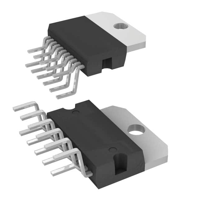
STMicroelectronics TDA7391LV
- Part No.:
- TDA7391LV
- Manufacturer:
- STMicroelectronics
- Category:
- Audio Amplifiers
- Package:
- Multiwatt-11 (Vertical, Bent and Staggered Leads)
- Datasheet:
-
 TDA7391LV.pdf
- Description:
- IC AMP AB MONO 45W MULTIWATT-11
- Quantity:
- Payment:

- Shipping:

Inventory:903
Please send an inquiry. Send us your inquiry, and we will respond immediately.
Product details
Overview
TDA7391LV from STMicroelectronics is a 40 W bridge-type Class AB audio power amplifier IC designed for automotive car radio systems, operating down to 6 V for start-stop and e-call compliance. It delivers 26 W into 4 Ω at 14.4 V/1 kHz/10% THD, features differential or single-ended inputs, integrated clipping detection, and CMOS-compatible standby control.
For engineers reviewing the TDA7391LV datasheet, TDA7391LV pinout, TDA7391LV application, or TDA7391LV equivalent, this page provides verified electrical specs, package mapping (Multiwatt 11), real-world low-voltage operation behavior, thermal protection details, and OEM-validated start-stop battery profile compatibility.
Technical Context
The TDA7391LV implements a fully complementary PNP/NPN output stage in bridge configuration, enabling rail-to-rail swing without bootstrap capacitors and supporting loads as low as 3.2 Ω. Its input stage accepts both differential and single-ended signals with matched impedance requirements (30–60 kΩ).
It integrates multiple protections: short-circuit (to GND, to VS, across load), overtemperature shutdown (160 °C), load dump tolerance (50 V peak), open-GND detection, and ESD hardening. The on-chip clipping detector (CD pin) outputs an open-collector low signal at ≥5% THD for external gain compression control.
Key Specifications
| Parameter | Value and Actual Design Meaning |
|---|---|
| Output Power | 40 W max into 4 Ω @ 14.4 V, 10% THD - enables high-fidelity mid-range audio in compact car head units |
| Supply Voltage Range | 6–18 V - supports full operation during engine cranking (6 V minimum) per OEM start-stop specifications |
| THD+N | 0.03% typ. @ 1 W, 4 Ω - ensures low distortion for critical listening environments |
| Input Impedance | 36–60 kΩ differential / 30–55 kΩ single-ended - minimizes loading on preceding preamp stages |
| Standby Current | ≤50 μA @ VST-BY = 1.5 V - enables ultra-low-power sleep mode for always-on infotainment systems |
| Clipping Detection Threshold | 5–15% THD - triggers CD pin for real-time gain limiting without external circuitry |
| Thermal Shutdown Temp | 160 °C junction - protects against sustained overload or poor heatsinking in enclosed dash environments |
Pinout & Package
Available in Multiwatt 11 (vertical) package with exposed metal tab for thermal dissipation (Rth j-case = 1.8 °C/W). Pin layout optimized for automotive PCB layout with dedicated signal ground (S-GND) and power ground (GND) separation.
| Pin/Terminal | Circuit Role | Design Meaning |
|---|---|---|
| 1, 2 | INPUTS | Differential input pair; accepts single-ended via AC coupling to GND - eliminates need for external phase-splitting circuitry |
| 3, 9 | +VS | Main supply input (6–18 V); handles 50 V transient peaks - compatible with 12 V automotive battery + load dump |
| 4 | CD | Open-collector clipping indicator - sinks current when THD ≥5%; used for automatic volume compression or LED alert |
| 5, 7 | OUTPUTS | Bridge outputs driving speaker directly - delivers full ±VS swing across load without DC blocking capacitors |
| 6 | GND | Power ground return for output stage and bias circuits - must be low-impedance path to chassis |
| 8 | STANDBY | CMOS-compatible enable pin; <1.5 V = standby (<50 μA ISB), >3.5 V = active - supports microcontroller GPIO control |
| 10 | SYNC | Timing pin for pop-free turn-on/off - sets soft-start ramp with external R-C network to suppress transients |
| 11 | MUTE | Mute timing control - internal capacitor-based delay prevents click/pop during power transitions |
| 12 | S-GND | Signal ground reference for inputs and feedback - isolated from power GND to reduce noise coupling |
Key Features
| Feature | Design Value |
|---|---|
| Low-voltage operation | Functional down to 6 V supply - meets ISO 16750-2 crank profile for start-stop engines without audio dropout |
| Integrated clipping detection | On-die THD monitoring with open-drain CD pin - enables adaptive loudness control without external ADC or comparator |
| Bridge output architecture | No output coupling capacitors required - reduces BOM count and avoids bass roll-off below 20 Hz |
| Multi-protection system | Single-chip coverage of short-circuit, overtemperature, load dump, and open-GND faults - eliminates need for discrete protection ICs |
| Dual ground separation | Dedicated S-GND and GND pins - suppresses ground loop noise in multi-channel head unit designs |
Applications
| Automotive Infotainment Head Unit | OEM Digital Radio Receiver |
|---|---|
|
Use Scenario: Integrated amplifier in 2-DIN car stereo supporting DAB+, HD Radio, and Bluetooth streaming. IC Role / Device Role / Timing Role: Final-stage bridge driver delivering 26 W/channel into 4 Ω speakers with THD <0.05% at 1 W. Use Value: Eliminates external mute logic and clipping feedback circuitry while maintaining OEM audio fidelity targets under 6–14.4 V battery variation. |
Use Scenario: Audio output stage in certified digital broadcast receiver module for European vehicle platforms. IC Role / Device Role / Timing Role: Low-noise, high-SVR amplifier accepting differential I²S DAC output with 65 dB CMRR at 1 kHz. Use Value: Meets stringent CISPR 25 Class 5 EMC requirements due to internal ground separation and fixed-gain architecture. |
| Start-Stop Compatible Navigation System | eCall Emergency Audio Module |
|
Use Scenario: Voice-guided navigation unit requiring uninterrupted audio during engine restart cycles. IC Role / Device Role / Timing Role: Amplifier sustaining playback at 4.2 W into 4 Ω even at 6 V supply, with <1.5% THD. Use Value: Maintains audible voice prompts during worst-case battery cranking (6 V for 50 ms) without reset or mute events. |
Use Scenario: Compact emergency call module with hands-free microphone and speaker interface. IC Role / Device Role / Timing Role: Single-channel 32 W amplifier driving 3.2 Ω speaker for loud cabin announcements. Use Value: Complies with UNECE R151 eCall acoustic output spec (≥65 dBA at 2 m) using only one IC and minimal passives. |
Equivalent & Alternatives
The following parts are listed as comparable options for similar audio power amplifier applications.
| Alternative Part | Technical Difference | Application Difference | Selection Advice |
|---|---|---|---|
| TDA7388 | Higher 4×50 W output, but requires ≥8 V min supply - no 6 V start-stop support | Targeted at premium non-start-stop head units; lacks integrated clipping detection | Select when higher channel count and power are needed, and battery profile allows ≥8 V operation |
| STA559BW | Digital input (I²S), Class D efficiency (90%), but larger QFN48 package and external gate drivers required | Used in connected-car platforms with DSP-based audio processing; not pin-compatible | Choose for thermally constrained layouts needing >85% efficiency and digital audio integration |
Compared with TDA7391LV, TDA7388 offers greater multi-channel power but sacrifices low-voltage robustness, while STA559BW delivers superior efficiency and digital interface at the cost of design complexity and footprint - making TDA7391LV optimal for cost-sensitive, analog-input, start-stop-compliant car radios.
Availability
TDA7391LV is available at Aetrix Electronics and suitable for automotive infotainment head units, OEM digital radio receivers, and start-stop compatible navigation systems requiring stable component supply across extended temperature ranges and long production lifecycles.
Supply support for TDA7391LV includes scheduled delivery planning, volume procurement assistance, BOM continuity management, traceable sourcing, and lifecycle availability coordination for OEM customers, industrial embedded developers, connected-device designers, and electronics production programs.
Manufacturer
STMicroelectronics is a global semiconductor leader headquartered in Geneva, Switzerland, specializing in automotive-grade analog, power, and microcontroller solutions with ISO/TS 16949-certified manufacturing.
The TDA7391LV belongs to ST's TDA7xxx automotive audio amplifier product line, engineered specifically for cost-optimized, high-reliability car radio applications demanding low-voltage resilience and integrated protection.
FAQ
What is the minimum supply voltage for continuous operation?
The TDA7391LV operates continuously down to 6 V, validated per ISO 16750-2 crank profiles for start-stop engines. At 6 V, it delivers 4.2 W into 4 Ω at 10% THD and remains fully functional with all protections active - no brown-out reset or latch-up occurs.
How does the clipping detection (CD) pin function in practice?
The CD pin is an open-collector output that pulls low when total harmonic distortion exceeds 5–15% (typ. 10%). It drives external LEDs or feeds back to a microcontroller to trigger automatic gain reduction, eliminating audible distortion during high-volume transients without added components.
Can the TDA7391LV drive 2 Ω loads?
No - the device is rated for minimum 3.2 Ω loads per the datasheet absolute maximum ratings and thermal derating curves. Driving 2 Ω would exceed safe operating area limits, triggering thermal shutdown or causing permanent damage due to excessive current (beyond 4.5 A peak).
Is the Multiwatt 11 package RoHS-compliant and lead-free?
Yes - the TDA7391LV Multiwatt 11 package carries ST's ECOPACK®2 certification, meeting RoHS Directive 2011/65/EU and JEDEC J-STD-609A Class 3 moisture sensitivity level, with lead-free terminations and halogen-free molding compound.
TDA7391LV Specifications
- Product attributes
- Attribute value
- Manufacturer:
- STMicroelectronics
- Series:
- -
- Package/Case:
- Multiwatt-11 (Vertical, Bent and Staggered Leads)
- Packaging:
- Tube
- Product Status:
- Active
- Type:
- Class AB
- Output Type:
- 1-Channel (Mono)
- Max Output Power x Channels @ Load:
- 45W x 1 @ 3.2Ohm
- Voltage - Supply:
- 6V ~ 18V
- Features:
- Depop, Differential Inputs, Mute, Short-Circuit and Thermal Protection, Standby
- Mounting Type:
- Through Hole
- Operating Temperature:
- -40°C ~ 150°C (TJ)
- Grade:
- -
- Qualification:
- -
- Supplier Device Package:
- Multiwatt-11 (Vertical, Bent and Staggered Leads)
TDA7391LV FAQ
1.How can I place an order for TDA7391LV through Aetrix?
Please submit a Request for Quotation (RFQ) for TDA7391LV on Aetrix. Our sales agent will provide a competitive quotation and guide you through the order confirmation once you accept the terms.
2.Are the price and stock information for TDA7391LV reliable?
The price and inventory of TDA7391LV are updated periodically and may fluctuate due to market conditions. Stock and pricing data are typically refreshed every 24 hours. Quotation validity for TDA7391LV is usually 5 days.
3.What payment methods are accepted for TDA7391LV?
We accept Wire Transfer, PayPal, Credit Card, Western Union, MoneyGram, and Escrow for TDA7391LV transactions.
Note: Certain payment methods may incur a processing fee.
4.How is shipping managed for TDA7391LV?
TDA7391LV orders can be shipped via leading logistics carriers, including DHL, UPS, FedEx, TNT, or Registered Mail.
Once your TDA7391LV order is processed, you will receive an email with the shipment details and tracking number.
Note: Tracking information may take up to 24 hours to appear. Express delivery typically takes 3–5 business days.
5.How can I obtain technical support or documentation for TDA7391LV?
For technical support, including TDA7391LV datasheets, pinout diagrams, or application guidance, please contact our engineering support team. They can provide detailed documentation and assistance for your TDA7391LV requirements.
6.How does Aetrix verify that TDA7391LV is sourced from the original manufacturer or authorized distributors?
All TDA7391LV products on Aetrix are procured from qualified distributors and authorized channels. Our dedicated quality assurance team conducts strict verification, including traceability checks and, if necessary, third-party testing. This ensures that TDA7391LV meets industry standards.
7.What is the process for return or replacement of TDA7391LV?
All TDA7391LV units undergo pre-shipment inspection (PSI). If there is an issue with TDA7391LV, returns or replacements are accepted under the following conditions:
1.Quantity discrepancies, incorrect items, or visible external defects (such as breakage or corrosion), acknowledged by Aetrix.
2.The issue is reported within 90 days of delivery.
3.The TDA7391LV part is unused and in its original packaging.
Return procedure for TDA7391LV:
1.Submit a request within 90 days.
2.Obtain a Return Material Authorization (RMA) from Aetrix.
TDA7391LV Tags
-Exposed-Pad.jpg)
-
TS34119CS RLG
Taiwan Semiconductor Corporation

-
LM386MX-1/NOPB
Texas Instruments

-
TPA711DGNR
Texas Instruments

-
LM386N-4/NOPB
Texas Instruments

-
TS4990IST
STMicroelectronics
-
PAM8302AASCR
Diodes Incorporated
-
TPA6130A2RTJR
Texas Instruments
-
TPA6111A2DGNR
Texas Instruments
-
LM4861MX/NOPB
Texas Instruments
-
LM386M-1/NOPB
Texas Instruments

-
NCS2211DR2G
onsemi
-
IS31AP2005-DLS2-TR
Lumissil Microsystems
Tech Hub

A practical engineering and sourcing framework covering lifecycle verification, lifetime-buy calculations, replacement qualification, supplier checks and counterfeit-risk controls.

TTL and CMOS logic families differ in thresholds, loading, output drive, power and timing. This engineering guide compares 74HC and 74HCT, calculates noise margins and checks 3.3 V/5 V compatibility.

A practical engineering guide to 3.3V and 5V logic compatibility, input thresholds, resistor dividers, translator ICs, MOSFET level shifting, I2C pull-ups, timing limits and power-sequencing risks.

The 74HC595 uses push-pull logic outputs, while the TPIC6B595 uses 50 V open-drain DMOS sinks for higher-power loads. This guide compares timing, current limits, 3.3 V interfacing, load wiring, thermal…

The 74HC595 converts serial data into eight stable parallel outputs. This guide covers pin functions, shift and storage timing, OE and MR behavior, drive-current limits, cascading, voltage compatibilit…

A technical comparison of level-sensitive latches and edge-triggered flip-flops, covering timing windows, setup and hold limits, master–slave operation, time borrowing, race-through, HDL inference and…

A D latch stores one bit while Enable controls when data can pass. This reference covers gate-level operation, truth tables, transparency, setup and hold timing, LE versus OE, common ICs and practical …

An SR latch stores one bit through cross-coupled feedback. This engineering reference covers NOR and NAND implementations, truth tables, forbidden-state recovery, gated operation, switch debouncing, fa…

Latch circuits retain one bit through feedback. This technical reference covers SR and D latches, truth tables, transparency, timing limits, latch-versus-flip-flop behavior, applications and common log…

An engineering guide to LED driver operation, constant-current and constant-voltage outputs, linear and switching topologies, dimming, IC selection, calculations, replacement compatibility, and fault c…


