
 My Inquiry
 My Account


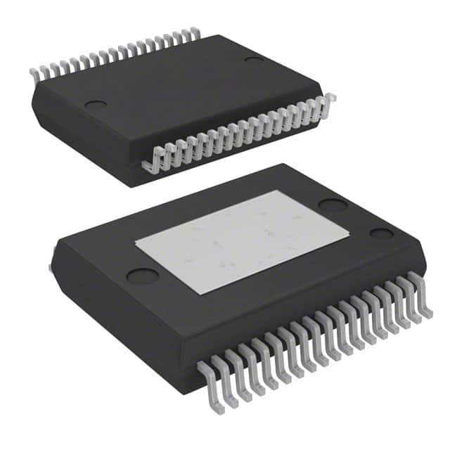
STMicroelectronics TDA7498L
- Part No.:
- TDA7498L
- Manufacturer:
- STMicroelectronics
- Category:
- Audio Amplifiers
- Package:
- 36-PowerFSOP (0.295", 7.50mm Width)
- Datasheet:
-
 TDA7498L.pdf
- Description:
- IC AMP D STEREO 80W POWERSSO36
- Quantity:
- Payment:

- Shipping:

Inventory:2,035
Please send an inquiry. Send us your inquiry, and we will respond immediately.
Product details
Overview
TDA7498L from STMicroelectronics is a dual-channel BTL Class-D audio amplifier IC designed for high-power active speaker and home theater systems. It delivers 80 W + 80 W into 6 Ω at 10% THD with 32 V supply, operates from a single 14–36 V rail, achieves 90% efficiency, and features four selectable fixed gains (25.6–37.6 dB) via digital inputs GAIN0/GAIN1.
For engineers reviewing the TDA7498L datasheet, TDA7498L pinout, TDA7498L application, or TDA7498L equivalent, key selection considerations include differential input noise immunity, thermal shutdown behavior at 150 °C, open-drain diagnostic output (pin 28), and external clock synchronization capability via SYNCLK for multi-amplifier systems.
Technical Context
The TDA7498L integrates two identical fully differential Class-D channels with internal PWM modulation, configurable switching frequency (250–400 kHz), and independent gain control per channel via GAIN0/GAIN1 logic inputs. Each channel uses separate power stage grounds (PGNDA/PGNDB), dedicated PVCC rails, and dual complementary PWM outputs (OUTPA/OUTNA, OUTPB/OUTNB).
It implements comprehensive protection: overcurrent (6 A threshold), overvoltage (42 V), undervoltage (8 V), and thermal shutdown (150 °C junction). Diagnostic status is reported via open-drain DIAG pin, while standby/mute modes are controlled by dedicated STBY and MUTE inputs with defined voltage thresholds (VSTBY_H ≥ 2.7 V, VMUTE_L ≤ 0.8 V).
Key Specifications
| Parameter | Value and Actual Design Meaning |
|---|---|
| Output power | 80 W + 80 W at THD = 10%, RL = 6 Ω, VCC = 32 V - enables high-fidelity stereo output without heatsink derating in compact enclosures |
| Supply range | 14–36 V single rail - supports wide-range DC bus operation in powered speakers and AV receivers |
| Efficiency | 90% typical at full output - minimizes thermal load and enables passive cooling in space-constrained designs |
| Gain settings | 25.6 / 31.6 / 35.1 / 37.6 dB - digitally selectable via GAIN0/GAIN1 to match source signal level and speaker sensitivity |
| THD+N | 0.1% typical at 1 W output - preserves audio fidelity across audible bandwidth (20 Hz–20 kHz) |
| Switching frequency | 290–330 kHz internal oscillator - allows use of small LC filter components (e.g., 22 µH + 680 nF for 8 Ω) |
| Input impedance | 60 kΩ differential - reduces loading on preceding DAC or line driver stages |
Pinout & Package
The TDA7498L is housed in a PowerSSO-36 exposed pad up (EPU) package with thermal pad connected to ground. The exposed pad (EP) provides low thermal resistance (Rth j-case = 2 °C/W typ.) and must be soldered to a heatsink or large copper area for reliable 80 W/channel operation.
| Pin/Terminal | Circuit Role | Design Meaning |
|---|---|---|
| OUTPA / OUTNA | Left channel BTL PWM outputs | Drive complementary signals to left speaker via LC filter; require symmetric layout to minimize EMI |
| OUTPB / OUTNB | Right channel BTL PWM outputs | Independent dual-output structure enables true stereo separation and channel isolation > 70 dB |
| INPA / INNA / INPB / INNB | Differential analog inputs | Reject common-mode noise from long cables; support balanced or single-ended input with AC coupling |
| GAIN0 / GAIN1 | Digital gain configuration inputs | Set closed-loop gain without external resistors; logic levels define four precise gain states |
| STBY / MUTE | Power management controls | STBY = L disables all circuitry (IqSTBY ≤ 10 µA); MUTE = L silences output while preserving bias (AMUTE ≥ 70 dB) |
| DIAG | Open-drain fault indicator | Pulled high externally; goes high-impedance during OCP/OVP/UVP/OTP - enables system-level fault logging |
| SYNCLK | Master/slave clock I/O | Configured as output (2×fSW) in master mode or input (fSW/2) in slave mode for synchronized multi-device operation |
| ROSC | Internal oscillator timing | Resistor value (e.g., 39 kΩ) sets fSW = 10⁶ / [(ROSC × 16 + 182) × 4] kHz - enables precise EMI tuning |
Key Features
| Feature | Design Value |
|---|---|
| Dual independent BTL channels | Each channel has dedicated PVCC, PGNDA/B, and differential inputs - eliminates crosstalk and enables asymmetric load driving |
| Thermal protection with mute recovery | Junction temperature >145 °C forces mute mode (50% duty cycle); >150 °C triggers shutdown - prevents permanent damage while maintaining partial functionality |
| External clock synchronization | SYNCLK pin supports master/slave topology - eliminates beat frequencies and intermodulation in multi-amplifier systems |
| Differential input architecture | 60 kΩ input resistance + common-mode rejection - suppresses noise from shared power supplies or adjacent digital circuits |
| Integrated 3.3 V regulators | VDDPW (power stage) and VDDS (signal blocks) provide clean, decoupled supplies - reduce need for external LDOs |
Applications
| Home Theater Receiver | Powered Studio Monitor |
|---|---|
|
Use Scenario: Integrated stereo amplification in compact AV receivers with HDMI audio return and DSP processing. IC Role / Device Role / Timing Role: Final power stage delivering amplified analog audio to front left/right speakers; synchronized via external clock to avoid jitter-induced distortion. Use Value: 90% efficiency reduces heat sink volume by >40% vs. Class-AB; differential inputs reject noise from adjacent video circuitry. |
Use Scenario: High-fidelity near-field monitoring in professional audio workstations with low-latency USB audio interfaces. IC Role / Device Role / Timing Role: Dual-channel Class-D output driver accepting balanced line-level input; gain configured to match interface output swing (2 Vrms). Use Value: 0.1% THD+N at 1 W ensures accurate tonal balance; thermal protection maintains stable output during extended calibration sessions. |
| Smart Soundbar | Multi-Zone Audio Distribution |
|
Use Scenario: Slim-profile soundbar with integrated DSP, Bluetooth, and voice assistant, requiring high output in minimal depth. IC Role / Device Role / Timing Role: Primary stereo amplifier driving full-range drivers; standby mode activated during voice assistant idle periods to cut quiescent current to <10 µA. Use Value: Single 24 V supply simplifies power architecture; exposed pad enables direct mounting to aluminum chassis for passive cooling. |
Use Scenario: Central audio hub distributing synchronized stereo signals to multiple rooms using daisy-chained amplifiers. IC Role / Device Role / Timing Role: Slave amplifier locked to master TDA7498L's SYNCLK output - ensures identical switching frequency across all zones. Use Value: Eliminates audible heterodyne tones between zones; DIAG pin feedback enables centralized fault reporting across distributed system. |
Equivalent & Alternatives
The following parts are listed as comparable options for similar dual-channel Class-D audio amplifier applications.
| Alternative Part | Technical Difference | Application Difference | Selection Advice |
|---|---|---|---|
| TAS5630B | Higher peak output (100 W + 100 W @ 6 Ω), but requires dual ±15 V supplies and lacks integrated 3.3 V regulators | Designed for industrial rack-mount amplifiers with forced-air cooling; no exposed-pad thermal path | Select when higher peak power and lower THD (<0.05%) are critical, and dual-supply infrastructure exists |
| MAX98357A | I²S digital input, 3.2 W/channel into 8 Ω, no differential analog inputs or external clock sync | Targeted at portable Bluetooth speakers with SoC-based audio processing; no protection diagnostics or high-voltage operation | Select for cost-sensitive, low-power embedded audio where digital interface and small footprint outweigh analog flexibility |
Compared with TAS5630B and MAX98357A, the TDA7498L uniquely balances high analog-input power (80 W/channel), single-supply simplicity (14–36 V), thermal robustness (exposed pad + OTP), and system-level coordination (SYNCLK + DIAG), making it optimal for mid-to-high-end powered audio products.
Availability
TDA7498L is available at Aetrix Electronics and suitable for home theater receivers, powered studio monitors, smart soundbars, and multi-zone audio distribution systems requiring stable component supply, long-term lifecycle support, and traceable sourcing.
Supply support for TDA7498L includes scheduled delivery planning, volume procurement assistance, BOM continuity management, traceable sourcing, and lifecycle availability coordination for OEM customers, industrial embedded developers, connected-device designers, and electronics production programs.
Manufacturer
STMicroelectronics is a global semiconductor leader headquartered in Geneva, Switzerland, specializing in analog, power, microcontrollers, and automotive ICs with strong emphasis on energy efficiency and industrial reliability.
The TDA7498L belongs to ST's high-power audio amplifier product line, engineered specifically for compact, thermally constrained consumer and pro-audio applications demanding high output, low distortion, and robust protection.
FAQ
What is the minimum recommended LC filter cutoff frequency for TDA7498L?
The LC filter cutoff frequency must exceed 22 kHz to preserve audio bandwidth while remaining significantly below the 250–400 kHz switching frequency to suppress EMI. For 6 Ω loads, ST recommends 22 µH inductors with 680 nF capacitors (cutoff ≈ 27 kHz); for 8 Ω, same inductor with 680 nF yields equivalent performance. Component parasitics must be minimized through tight layout.
How does the TDA7498L handle thermal overload during continuous high-power operation?
At 145 °C junction temperature, the device enters mute mode (50% PWM duty cycle) to reduce power dissipation while maintaining bias; if temperature reaches 150 °C, it shuts down completely and forces outputs to high-impedance. Recovery is automatic once junction cools below 140 °C. The exposed pad and Rth j-case = 2 °C/W enable rapid heat transfer to external heatsinks.
Can TDA7498L operate with a single-ended input instead of differential?
Yes - the differential inputs (INPA/INNA, INPB/INNB) accept single-ended signals by grounding the negative input (e.g., INNA or INNB) and applying the signal to the positive input. Input impedance remains ~60 kΩ, and common-mode rejection is forfeited, but THD and SNR remain within spec for most consumer applications. AC coupling capacitors (≥470 nF) are mandatory.
What happens to the DIAG pin during undervoltage protection activation?
During undervoltage protection (VCC < 8 V), the DIAG pin transitions from low (active pull-down) to high-impedance (open-drain off), signaling fault condition to an external microcontroller or LED driver. This behavior is identical for overvoltage, overcurrent, and thermal shutdown events. A 10 kΩ pull-up to 3.3 V is recommended for clean logic-level detection.
TDA7498L Specifications
- Product attributes
- Attribute value
- Manufacturer:
- STMicroelectronics
- Series:
- -
- Package/Case:
- 36-PowerFSOP (0.295", 7.50mm Width)
- Packaging:
- Tube
- Product Status:
- Obsolete
- Type:
- Class D
- Output Type:
- 2-Channel (Stereo)
- Max Output Power x Channels @ Load:
- 80W x 2 @ 6Ohm
- Voltage - Supply:
- 14V ~ 36V
- Features:
- Differential Inputs, Mute, Short-Circuit and Thermal Protection, Standby
- Mounting Type:
- Surface Mount
- Operating Temperature:
- -40°C ~ 85°C (TA)
- Grade:
- -
- Qualification:
- -
- Supplier Device Package:
- PowerSSO-36 EPU
TDA7498L FAQ
1.How can I place an order for TDA7498L through Aetrix?
Please submit a Request for Quotation (RFQ) for TDA7498L on Aetrix. Our sales agent will provide a competitive quotation and guide you through the order confirmation once you accept the terms.
2.Are the price and stock information for TDA7498L reliable?
The price and inventory of TDA7498L are updated periodically and may fluctuate due to market conditions. Stock and pricing data are typically refreshed every 24 hours. Quotation validity for TDA7498L is usually 5 days.
3.What payment methods are accepted for TDA7498L?
We accept Wire Transfer, PayPal, Credit Card, Western Union, MoneyGram, and Escrow for TDA7498L transactions.
Note: Certain payment methods may incur a processing fee.
4.How is shipping managed for TDA7498L?
TDA7498L orders can be shipped via leading logistics carriers, including DHL, UPS, FedEx, TNT, or Registered Mail.
Once your TDA7498L order is processed, you will receive an email with the shipment details and tracking number.
Note: Tracking information may take up to 24 hours to appear. Express delivery typically takes 3–5 business days.
5.How can I obtain technical support or documentation for TDA7498L?
For technical support, including TDA7498L datasheets, pinout diagrams, or application guidance, please contact our engineering support team. They can provide detailed documentation and assistance for your TDA7498L requirements.
6.How does Aetrix verify that TDA7498L is sourced from the original manufacturer or authorized distributors?
All TDA7498L products on Aetrix are procured from qualified distributors and authorized channels. Our dedicated quality assurance team conducts strict verification, including traceability checks and, if necessary, third-party testing. This ensures that TDA7498L meets industry standards.
7.What is the process for return or replacement of TDA7498L?
All TDA7498L units undergo pre-shipment inspection (PSI). If there is an issue with TDA7498L, returns or replacements are accepted under the following conditions:
1.Quantity discrepancies, incorrect items, or visible external defects (such as breakage or corrosion), acknowledged by Aetrix.
2.The issue is reported within 90 days of delivery.
3.The TDA7498L part is unused and in its original packaging.
Return procedure for TDA7498L:
1.Submit a request within 90 days.
2.Obtain a Return Material Authorization (RMA) from Aetrix.
TDA7498L Tags
-Exposed-Pad.jpg)
-
TS34119CS RLG
Taiwan Semiconductor Corporation

-
LM386MX-1/NOPB
Texas Instruments

-
TPA711DGNR
Texas Instruments

-
LM386N-4/NOPB
Texas Instruments

-
TS4990IST
STMicroelectronics
-
PAM8302AASCR
Diodes Incorporated
-
TPA6130A2RTJR
Texas Instruments
-
TPA6111A2DGNR
Texas Instruments
-
LM4861MX/NOPB
Texas Instruments
-
LM386M-1/NOPB
Texas Instruments

-
NCS2211DR2G
onsemi
-
IS31AP2005-DLS2-TR
Lumissil Microsystems
Tech Hub

A practical engineering and sourcing framework covering lifecycle verification, lifetime-buy calculations, replacement qualification, supplier checks and counterfeit-risk controls.

TTL and CMOS logic families differ in thresholds, loading, output drive, power and timing. This engineering guide compares 74HC and 74HCT, calculates noise margins and checks 3.3 V/5 V compatibility.

A practical engineering guide to 3.3V and 5V logic compatibility, input thresholds, resistor dividers, translator ICs, MOSFET level shifting, I2C pull-ups, timing limits and power-sequencing risks.

The 74HC595 uses push-pull logic outputs, while the TPIC6B595 uses 50 V open-drain DMOS sinks for higher-power loads. This guide compares timing, current limits, 3.3 V interfacing, load wiring, thermal…

The 74HC595 converts serial data into eight stable parallel outputs. This guide covers pin functions, shift and storage timing, OE and MR behavior, drive-current limits, cascading, voltage compatibilit…

A technical comparison of level-sensitive latches and edge-triggered flip-flops, covering timing windows, setup and hold limits, master–slave operation, time borrowing, race-through, HDL inference and…

A D latch stores one bit while Enable controls when data can pass. This reference covers gate-level operation, truth tables, transparency, setup and hold timing, LE versus OE, common ICs and practical …

An SR latch stores one bit through cross-coupled feedback. This engineering reference covers NOR and NAND implementations, truth tables, forbidden-state recovery, gated operation, switch debouncing, fa…

Latch circuits retain one bit through feedback. This technical reference covers SR and D latches, truth tables, transparency, timing limits, latch-versus-flip-flop behavior, applications and common log…

An engineering guide to LED driver operation, constant-current and constant-voltage outputs, linear and switching topologies, dimming, IC selection, calculations, replacement compatibility, and fault c…


