
 My Inquiry
 My Account


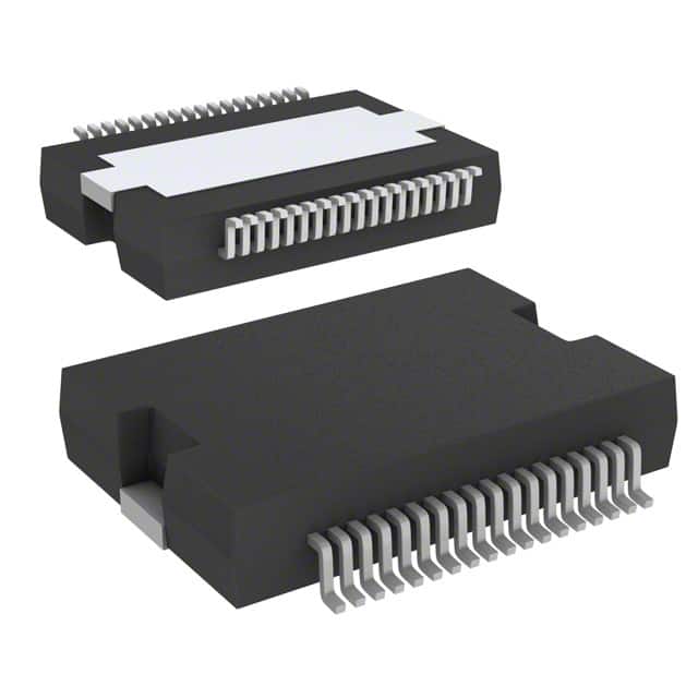
STMicroelectronics TDA75610S-ZST
- Part No.:
- TDA75610S-ZST
- Manufacturer:
- STMicroelectronics
- Category:
- Audio Amplifiers
- Package:
- PowerSO-36 Exposed Bottom Pad
- Datasheet:
-
 TDA75610S-ZST.pdf
- Description:
- IC AMP AB QUAD 45W POWERSO-36
- Quantity:
- Payment:

- Shipping:

Inventory:1,331
Please send an inquiry. Send us your inquiry, and we will respond immediately.
Product details
Overview
TDA75610S-ZST from STMicroelectronics is a quad-channel Class SB automotive audio power amplifier in PowerSO36 package, delivering up to 4 × 45 W into 4 Ω at 14.4 V with 10% THD, full I²C diagnostics (DC/AC load detection, fault reporting), and operation down to 6 V for start-stop systems.
For engineers reviewing the TDA75610S-ZST datasheet, TDA75610S-ZST pinout, TDA75610S-ZST application, or TDA75610S-ZST equivalent, this device supports robust speaker-level diagnostics, selectable 26 dB/16 dB gain, thermal warning thresholds, clipping detection with 1%/2% threshold options, and dual-mode efficiency control for low-power listening and high-output demand scenarios.
Technical Context
The TDA75610S-ZST implements ST's patented Class SB architecture-combining BCD process MOSFET output stages with adaptive biasing to reduce quiescent dissipation while maintaining linearity. It integrates four independent bridge outputs, each with dedicated short-circuit protection, DC offset detection, and thermal foldback.
I²C communication enables real-time status reporting per channel (e.g., open-load, short-to-GND, short-to-VCC, thermal warnings), configurable via address-select pins and programmable registers. The device supports legacy analog control (STBY/MUTE pins) alongside digital command sets for soft play/mute, gain selection, and diagnostic enable/disable.
Key Specifications
| Parameter | Value and Actual Design Meaning |
|---|---|
| Output Power | 4 × 45 W max into 4 Ω @ 14.4 V, 10% THD - enables high-fidelity rear/surround channel amplification without external heatsink oversizing |
| Supply Voltage Range | 6–18 V - supports engine cranking (6 V) and battery transients (up to 28 V absolute max), critical for start-stop compliance |
| THD+N | 0.015% typ. @ 1 W, 1 kHz, 4 Ω - ensures low-noise cabin audio reproduction with minimal harmonic distortion |
| I²C Diagnostics | Per-channel DC/AC load detection, thermal warnings (THWARN1–THWARN3), and fault latching - eliminates need for external monitoring circuitry |
| Clipping Detection | Selectable 1% or 2% THD threshold via IB1 register - allows precise signal integrity monitoring for dynamic range optimization |
| Thermal Resistance | Rth(j-case) = 1 °C/W (PowerSO36) - enables compact PCB layout with direct slug thermal coupling to heatsink |
| Standby Current | 1 µA typ. - meets OEM requirements for ultra-low quiescent consumption during vehicle sleep mode |
Pinout & Package
Package: PowerSO36 (slug-up, exposed thermal pad). Pin count: 36 terminals. Thermal performance optimized for automotive under-dash mounting with direct heatsink contact.
| Pin/Terminal | Circuit Role | Design Meaning |
|---|---|---|
| TAB (Pin 1) | Exposed thermal pad | Primary heat path to PCB/heatsink; must be soldered to copper pour for Rth(j-case) ≤ 1 °C/W |
| OUT1+ to OUT4− (Pins 2,4,8,10,16–17,19,22,33,34,36) | Differential speaker outputs | Four fully independent bridge outputs; each capable of driving 2 Ω loads (64 W peak) with integrated current limiting |
| CK / DATA / ADSEL (Pins 3,7,9) | I²C interface + configuration | Standard I²C clock/data lines; ADSEL sets slave address (0x48/0x49) and disables I²C when pulled high |
| STBY (Pin 11) | Hardware standby control | Logic-level input: <1.2 V = standby (90 dB attenuation), >4.5 V = active - supports fail-safe mute on microcontroller reset |
| CD (Pin 16) | Clipping detector output | Open-drain flag asserted when output THD exceeds programmed threshold (1% or 2%) - feeds MCU interrupt or LED indicator |
| SVR (Pin 24) | Supply voltage rejection enhancement | Connects to external capacitor to suppress battery ripple-induced noise during cranking (e.g., 100 µF ceramic) |
Key Features
| Feature | Design Value |
|---|---|
| Class SB Efficiency Architecture | Reduces average dissipation by ~40% vs. Class AB at typical listening levels - extends thermal margin and enables smaller heatsinks |
| Per-Channel Fault Isolation | Four independent short-circuit protections plus DC offset detection - prevents single-channel failure from disabling entire amplifier |
| Start-Stop Low-Voltage Operation | Stable 4 × 25 W output at 6 V supply - maintains cabin audio functionality during engine stop without brownout or mute events |
| I²C Diagnostic Reporting | Real-time readout of speaker impedance, thermal state, clipping status, and fault history - replaces discrete sense resistors and comparators |
| Robust Misconnection Tolerance | Withstands reverse-battery, output short-to-ground/VCC, and floating inputs - reduces field return rates in production vehicles |
Applications
| Infotainment Head Unit Amplifier | Active Noise Cancellation (ANC) Driver |
|---|---|
Use Scenario: Integrated 4-channel amplifier in OEM head unit providing front/rear speaker drive with digital audio processing. IC Role / Device Role / Timing Role: Final-stage power driver with I²C-configurable gain and real-time speaker health reporting. Use Value: Eliminates need for external diagnostic ICs and reduces BOM count by consolidating protection, clipping detection, and thermal management into one die. | Use Scenario: Driving error speakers in vehicle cabin ANC systems requiring low-latency, low-distortion analog output. IC Role / Device Role / Timing Role: High-fidelity, low-THD (<0.02%) analog output stage synchronized to DSP-generated anti-noise waveforms. Use Value: 22 kHz bandwidth and 70 dB CMRR suppress reference signal leakage, ensuring clean error speaker actuation without feedback oscillation. |
| Start-Stop Compliant Audio Module | Aftermarket DSP Integration Amplifier |
Use Scenario: Audio subsystem in hybrid/electric vehicles where battery voltage drops to 6 V during engine stop. IC Role / Device Role / Timing Role: Primary power amplifier maintaining rated output power and stability across 6–16 V supply range. Use Value: No audible dropout or muting during cranking; SVR pin filtering suppresses 100 Hz–10 kHz battery ripple without external regulators. | Use Scenario: External amplifier module receiving processed signals from aftermarket DSP units via line-level inputs. IC Role / Device Role / Timing Role: High-input-impedance (60 kΩ) analog receiver with selectable 16 dB/26 dB gain to match DSP output swing. Use Value: Gain-matching flexibility avoids signal clipping in downstream stages; ESD-protected inputs tolerate hot-plug connection to DSP boards. |
Equivalent & Alternatives
The following parts are listed as comparable options for similar quad-channel automotive amplifier applications.
| Alternative Part | Technical Difference | Application Difference | Selection Advice |
|---|---|---|---|
| TDA75610S-QLX | Same silicon, Flexiwatt27 horizontal package - larger footprint, higher Rth(j-case) (1.2 °C/W), no exposed thermal slug | Preferred for through-hole prototyping or legacy board reuse; less suitable for high-power density designs | Select when mechanical compatibility with existing Flexiwatt layouts is required and thermal budget allows 15–20% lower power derating |
| TDA75610S-ZSX | Same silicon, PowerSO36 tube-packaged variant - identical electrical specs and thermal performance, different logistics packaging | No functional difference; used for manual assembly or small-batch builds where tape-and-reel is not needed | Choose for engineering samples or low-volume production where reel handling infrastructure is unavailable |
Compared with TDA75610S-QLX and TDA75610S-ZSX, the TDA75610S-ZST offers identical core functionality but optimizes for automated SMT placement and maximum thermal efficiency via tape-and-reel delivery-making it the preferred choice for high-volume automotive Tier-1 manufacturing.
Availability
TDA75610S-ZST is available at Aetrix Electronics and suitable for automotive infotainment systems, start-stop compliant audio modules, and aftermarket DSP-integrated amplifiers requiring stable component supply, long lifecycle support, and AEC-Q100 qualified parts.
Supply support for TDA75610S-ZST includes scheduled delivery planning, volume procurement assistance, BOM continuity management, traceable sourcing, and lifecycle availability coordination for OEM customers, industrial embedded developers, connected-device designers, and electronics production programs.
Manufacturer
STMicroelectronics is a global semiconductor leader headquartered in Geneva, specializing in automotive-grade analog, power, and microcontroller solutions with over 30 years of OEM qualification experience.
The TDA75610S-ZST belongs to ST's TDA75xx family of intelligent Class SB audio amplifiers-designed specifically for next-generation automotive audio systems demanding high efficiency, comprehensive diagnostics, and robust low-voltage operation.
FAQ
What is the minimum supply voltage for full 4 × 25 W output capability?
The TDA75610S-ZST delivers 4 × 25 W into 4 Ω at 10% THD with a minimum supply of 6 V, verified per Table 5 in the datasheet (DocID025599 Rev 6). This enables uninterrupted audio playback during engine cranking and start-stop cycles without gain reduction or muting.
How does the I²C diagnostic system report speaker faults?
The I²C bus provides per-channel status registers indicating open-load, short-to-GND, short-to-VCC, thermal warnings (THWARN1–THWARN3), and clipping events. Each fault is latched and readable via standard I²C read commands to addresses 0x48 or 0x49, depending on ADSEL pin state.
Can the clipping detector threshold be changed dynamically during operation?
Yes-the clipping threshold is set via the IB1 register (bit D7) and can be modified in real time over I²C. Setting IB1 = 1 selects 10% THD detection; IB1 = 0 selects 2% THD detection. No hardware reconfiguration or power cycle is required.
Is the PowerSO36 package RoHS and AEC-Q100 qualified?
Yes-the TDA75610S-ZST in PowerSO36 packaging is qualified to AEC-Q100 Grade 2 (−40 °C to +105 °C ambient) and complies with RoHS Directive 2011/65/EU. Qualification data is documented in ST's official product change notices and reliability reports.
TDA75610S-ZST Specifications
- Product attributes
- Attribute value
- Manufacturer:
- STMicroelectronics
- Series:
- -
- Package/Case:
- PowerSO-36 Exposed Bottom Pad
- Packaging:
- Tape & Reel (TR)
- Product Status:
- Active
- Type:
- Class AB
- Output Type:
- 4-Channel (Quad)
- Max Output Power x Channels @ Load:
- 45W x 4 @ 4Ohm
- Voltage - Supply:
- 6V ~ 18V
- Features:
- Mute, Standby
- Mounting Type:
- Surface Mount
- Operating Temperature:
- -40°C ~ 105°C (TA)
- Grade:
- -
- Qualification:
- -
- Supplier Device Package:
- PowerSO-36
TDA75610S-ZST FAQ
1.How can I place an order for TDA75610S-ZST through Aetrix?
Please submit a Request for Quotation (RFQ) for TDA75610S-ZST on Aetrix. Our sales agent will provide a competitive quotation and guide you through the order confirmation once you accept the terms.
2.Are the price and stock information for TDA75610S-ZST reliable?
The price and inventory of TDA75610S-ZST are updated periodically and may fluctuate due to market conditions. Stock and pricing data are typically refreshed every 24 hours. Quotation validity for TDA75610S-ZST is usually 5 days.
3.What payment methods are accepted for TDA75610S-ZST?
We accept Wire Transfer, PayPal, Credit Card, Western Union, MoneyGram, and Escrow for TDA75610S-ZST transactions.
Note: Certain payment methods may incur a processing fee.
4.How is shipping managed for TDA75610S-ZST?
TDA75610S-ZST orders can be shipped via leading logistics carriers, including DHL, UPS, FedEx, TNT, or Registered Mail.
Once your TDA75610S-ZST order is processed, you will receive an email with the shipment details and tracking number.
Note: Tracking information may take up to 24 hours to appear. Express delivery typically takes 3–5 business days.
5.How can I obtain technical support or documentation for TDA75610S-ZST?
For technical support, including TDA75610S-ZST datasheets, pinout diagrams, or application guidance, please contact our engineering support team. They can provide detailed documentation and assistance for your TDA75610S-ZST requirements.
6.How does Aetrix verify that TDA75610S-ZST is sourced from the original manufacturer or authorized distributors?
All TDA75610S-ZST products on Aetrix are procured from qualified distributors and authorized channels. Our dedicated quality assurance team conducts strict verification, including traceability checks and, if necessary, third-party testing. This ensures that TDA75610S-ZST meets industry standards.
7.What is the process for return or replacement of TDA75610S-ZST?
All TDA75610S-ZST units undergo pre-shipment inspection (PSI). If there is an issue with TDA75610S-ZST, returns or replacements are accepted under the following conditions:
1.Quantity discrepancies, incorrect items, or visible external defects (such as breakage or corrosion), acknowledged by Aetrix.
2.The issue is reported within 90 days of delivery.
3.The TDA75610S-ZST part is unused and in its original packaging.
Return procedure for TDA75610S-ZST:
1.Submit a request within 90 days.
2.Obtain a Return Material Authorization (RMA) from Aetrix.
TDA75610S-ZST Tags
-Exposed-Pad.jpg)
-
TS34119CS RLG
Taiwan Semiconductor Corporation

-
LM386MX-1/NOPB
Texas Instruments

-
TPA711DGNR
Texas Instruments

-
LM386N-4/NOPB
Texas Instruments

-
TS4990IST
STMicroelectronics
-
PAM8302AASCR
Diodes Incorporated
-
TPA6130A2RTJR
Texas Instruments
-
TPA6111A2DGNR
Texas Instruments
-
LM4861MX/NOPB
Texas Instruments
-
LM386M-1/NOPB
Texas Instruments

-
NCS2211DR2G
onsemi
-
IS31AP2005-DLS2-TR
Lumissil Microsystems
Tech Hub

A practical engineering and sourcing framework covering lifecycle verification, lifetime-buy calculations, replacement qualification, supplier checks and counterfeit-risk controls.

TTL and CMOS logic families differ in thresholds, loading, output drive, power and timing. This engineering guide compares 74HC and 74HCT, calculates noise margins and checks 3.3 V/5 V compatibility.

A practical engineering guide to 3.3V and 5V logic compatibility, input thresholds, resistor dividers, translator ICs, MOSFET level shifting, I2C pull-ups, timing limits and power-sequencing risks.

The 74HC595 uses push-pull logic outputs, while the TPIC6B595 uses 50 V open-drain DMOS sinks for higher-power loads. This guide compares timing, current limits, 3.3 V interfacing, load wiring, thermal…

The 74HC595 converts serial data into eight stable parallel outputs. This guide covers pin functions, shift and storage timing, OE and MR behavior, drive-current limits, cascading, voltage compatibilit…

A technical comparison of level-sensitive latches and edge-triggered flip-flops, covering timing windows, setup and hold limits, master–slave operation, time borrowing, race-through, HDL inference and…

A D latch stores one bit while Enable controls when data can pass. This reference covers gate-level operation, truth tables, transparency, setup and hold timing, LE versus OE, common ICs and practical …

An SR latch stores one bit through cross-coupled feedback. This engineering reference covers NOR and NAND implementations, truth tables, forbidden-state recovery, gated operation, switch debouncing, fa…

Latch circuits retain one bit through feedback. This technical reference covers SR and D latches, truth tables, transparency, timing limits, latch-versus-flip-flop behavior, applications and common log…

An engineering guide to LED driver operation, constant-current and constant-voltage outputs, linear and switching topologies, dimming, IC selection, calculations, replacement compatibility, and fault c…


