
 My Inquiry
 My Account


Infineon Technologies TLE9832QVXUMA3
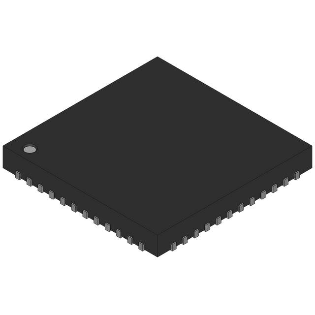
- Part No.:
- TLE9832QVXUMA3
- Manufacturer:
- Infineon Technologies
- Category:
- Application Specific Microcontrollers
- Package:
- 48-VFQFN Exposed Pad
- Datasheet:
-
 TLE9832QVXUMA3.pdf
- Description:
- IC MOTOR DRIVER 48VQFN
- Quantity:
- Payment:

- Shipping:

Inventory:2,793
Please send an inquiry. Send us your inquiry, and we will respond immediately.
Product details
Overview
TLE9832QVXUMA3 from Infineon Technologies is an automotive-qualified 8-bit microcontroller integrating LIN transceiver, dual low-side switches (1.2 A continuous), one high-side switch (0.5 A), 32 kB Flash + 4 kB emulated EEPROM, XC800 core (40 MHz), and 10-bit ADC - designed for body control modules, seat/mirror actuators, and LIN-connected smart sensors.
For engineers reviewing the TLE9832QVXUMA3 datasheet, TLE9832QVXUMA3 pinout, TLE9832QVXUMA3 application, or TLE9832QVXUMA3 equivalent, this device delivers integrated power switching, LIN 2.1 compliance, fail-safe clock monitoring, on-chip 1.5 V core regulation, and debug via 2-wire DAP - critical for cost-sensitive, space-constrained automotive subsystems requiring functional safety support.
Technical Context
The TLE9832QVXUMA3 integrates a 40 MHz XC800 8051-compatible core with two data pointers and two clocks per machine cycle, enabling deterministic real-time control. Its PMU provides independent 1.5 V (VDDC) core and 5.0 V (VDDP) I/O supplies, plus external 5.0 V regulator input (VDDEXT) for system-level power flexibility.
Functional integration includes LIN 2.1-compliant transceiver with wake-up capability, CCU6-based PWM generation with dead-time control, dual low-side switches with overcurrent clamping and PWM modulation, and a high-side switch with cyclic current sense for load diagnostics - all coordinated under a single system control unit with watchdog windowing and loss-of-clock detection.
Key Specifications
| Parameter | Value and Actual Design Meaning |
|---|---|
| Core | XC800 8051-compatible, 40 MHz max, 2-cycle instruction execution - enables fast response in motor control loops and LIN protocol timing. |
| Memory | 32 kB Flash + 4 kB emulated EEPROM, 256 B RAM, 3 kB XRAM - supports firmware updates, parameter storage, and runtime data buffering without external memory. |
| LIN Interface | LIN 1.3/2.0/2.1 compliant transceiver with wake-up detection - eliminates need for discrete LIN PHY and reduces BOM count in distributed nodes. |
| Power Switches | 2× Low-side switches (1.2 A continuous, clamped), 1× High-side switch (0.5 A, cyclic sense) - enables direct driving of relays, solenoids, and LEDs with built-in diagnostics. |
| ADC | 10-bit SAR ADC with 8 channels, VAREF reference, ±1 LSB INL - suitable for battery voltage monitoring, temperature sensing, and potentiometer feedback in automotive environments. |
| Timers & PWM | Five 16-bit timers + CCU6 capture/compare unit - supports multi-channel PWM generation with programmable dead time for BLDC commutation or lamp dimming. |
| Debug | 2-wire Device Access Port (DAP) - enables in-system programming and real-time debugging with minimal pin overhead and no SWD/JTAG header required. |
Pinout & Package
Package: QFN-48 (7 mm × 7 mm, 0.5 mm pitch) with exposed thermal pad - optimized for compact automotive PCB layouts and thermal dissipation in sealed enclosures.
| Pin/Terminal | Circuit Role | Design Meaning |
|---|---|---|
| VDDP | I/O Supply Voltage | 5.0 V regulated supply for GPIO, LIN transceiver, and peripheral logic - must be decoupled with ≥1 µF ceramic capacitor near pin. |
| VDDC | Core Supply Voltage | 1.5 V regulated supply for XC800 core - generated internally; external bypass required at VDDC pin for stability. |
| VDDEXT | External 5.0 V Regulator Input | Input for external 5.0 V regulator to power VDDP - used when internal VDDP regulator is disabled or insufficient. |
| HSW | High-Side Switch Output | Drives loads between VBAT and HSW pin; supports cyclic current sense for open-load and short-circuit detection. |
| LSW1 / LSW2 | Low-Side Switch Outputs | Ground-switched outputs with active clamping; each supports PWM up to 20 kHz and overcurrent shutdown with auto-recovery. |
| LIN | LIN Bus Transceiver I/O | Single-wire bidirectional LIN bus interface compliant to ISO 17987-4; includes wake-up pulse detection and slew-rate control. |
| XTAL1 / XTAL2 | Crystal Oscillator Inputs | Supports 1–20 MHz crystal or external clock source; PLL locks to generate stable 40 MHz system clock with loss-of-clock detection. |
Key Features
| Feature | Design Value |
|---|---|
| Integrated LIN Transceiver | LIN 2.1 compliance with wake-up, bus short-circuit protection, and ESD tolerance >2 kV HBM - reduces external component count and improves node robustness. |
| Fail-Safe Clock Monitoring | Dedicated loss-of-clock detection circuit triggers automatic fail-safe mode for power switches - prevents uncontrolled actuator movement during oscillator failure. |
| On-Chip Power Switch Diagnostics | Cyclic current sense on HSW and clamping on LSWs enable real-time load fault detection (open, short, overtemp) without external sense resistors or op-amps. |
| BootROM with LIN BSL | Pre-programmed boot ROM supports LIN Bootstrap Loader - allows field firmware updates over LIN bus without dedicated programming hardware. |
| 2-Wire DAP Debug | Single-pin debug interface with full flash read/write and breakpoint support - simplifies production test and field diagnostics while saving PCB space. |
Applications
| Seat Position Control | Mirror Adjustment Module |
|---|---|
|
Use Scenario: Motorized adjustment of automotive seat fore/aft, recline, and lumbar positions using DC motors and potentiometer feedback. IC Role / Device Role / Timing Role: Central controller executing position PID loops, interpreting LIN commands from body domain controller, and driving H-bridge via LSW1/LSW2 PWM outputs. Use Value: Integrated low-side switches eliminate external driver ICs; LIN transceiver enables plug-and-play integration into vehicle LIN topology without gateway translation. |
Use Scenario: Bidirectional control of side-view mirror tilt and fold functions with end-stop detection and anti-pinch behavior. IC Role / Device Role / Timing Role: LIN slave node receiving position commands, managing motor direction/speed via CCU6 PWM, and monitoring current sense for stall detection. Use Value: Cyclic high-side sense on HSW enables accurate motor current measurement for anti-pinch torque limiting - no external shunt or amplifier required. |
| Smart Window Lift Controller | Body Control Relay Driver |
|
Use Scenario: One-touch auto-up/down window control with obstacle detection, battery voltage compensation, and LIN-synchronized status reporting. IC Role / Device Role / Timing Role: Real-time motor control unit sampling ADC for voltage/current, executing safety algorithms, and communicating status via LIN transceiver. Use Value: On-chip 10-bit ADC and 40 MHz core enable precise speed profiling and fast reaction to current spikes - meeting OEM anti-pinch timing requirements (<150 ms). |
Use Scenario: Centralized relay driving for lighting, HVAC actuators, and accessory power distribution in entry-level BCMs. IC Role / Device Role / Timing Role: LIN slave executing relay ON/OFF commands, monitoring coil voltage and contact state via ADC inputs and HSW sense. Use Value: Dual LSWs drive relays directly; integrated VBAT_SENSE attenuator enables accurate battery monitoring for load shedding decisions during cranking. |
Equivalent & Alternatives
The following parts are listed as comparable options for similar automotive microcontroller-with-integrated-power-switch applications.
| Alternative Part | Technical Difference | Application Difference | Selection Advice |
|---|---|---|---|
| TLF35584QVVS1 | Dedicated system basis chip (SBC) with 3x LDOs, watchdog, and CAN/LIN transceivers - no MCU core or embedded Flash. | Used as companion power/communication IC alongside separate MCU (e.g., SAK-TC275); lacks integrated control logic. | Select when higher ASIL-B functional safety certification, CAN interface, or multi-rail power management is required - not a drop-in replacement. |
| SPC560B50L5 | 32-bit Power Architecture MCU (64 MHz), 512 kB Flash, no integrated power switches - requires external half-bridge drivers and LIN transceiver. | Suitable for higher-performance body control or gateway applications needing CAN FD and larger code footprint. | Choose for scalable architecture where future feature expansion (e.g., OTA updates, secure boot) justifies added BOM complexity and cost. |
Compared with TLF35584QVVS1 and SPC560B50L5, the TLE9832QVXUMA3 uniquely combines 8-bit real-time control, LIN connectivity, and dual low-side/high-side switching in a single QFN-48 package - delivering lowest system cost and smallest footprint for LIN-actuated body electronics below 100 kHz PWM bandwidth.
Availability
TLE9832QVXUMA3 is available at Aetrix Electronics and suitable for seat position control, mirror adjustment modules, smart window lift controllers, and body control relay drivers requiring stable component supply across automotive production lifecycles.
Supply support for TLE9832QVXUMA3 includes scheduled delivery planning, volume procurement assistance, BOM continuity management, traceable sourcing, and lifecycle availability coordination for OEM customers, industrial embedded developers, connected-device designers, and electronics production programs.
Manufacturer
Infineon Technologies AG is a German semiconductor manufacturer specializing in power management, automotive MCUs, and sensor solutions - with global R&D centers and automotive-grade manufacturing facilities certified to IATF 16949.
The TLE9832 belongs to Infineon's TLE98xx family of automotive LIN system-on-chip devices - engineered specifically for cost-optimized, functionally safe body electronics where integration of control, communication, and power switching reduces system complexity and validation effort.
FAQ
Does TLE9832QVXUMA3 support LIN 2.1 physical layer and protocol stack?
Yes, the integrated LIN transceiver complies with LIN 2.1 (ISO 17987-4), including slew-rate control, bus short-circuit protection, and wake-up pulse detection. The on-chip BootROM includes LIN Bootstrap Loader (LIN BSL) firmware, enabling firmware updates over LIN without external tools - verified in Infineon's TLE9832 Application Note AP32277.
What is the maximum continuous current rating for the integrated high-side switch?
The high-side switch (HSW) supports 0.5 A continuous current at ambient temperatures up to 125 °C, with thermal shutdown activation at junction temperatures exceeding 160 °C. Current limit is fixed at 1.2 A peak, and cyclic sense enables diagnostic reporting of load current every 100 µs - specified in Section 5.11 of the Rev. 1.1 datasheet.
Can the TLE9832QVXUMA3 operate without an external crystal?
Yes - it includes an internal RC oscillator (12 MHz ±10%) usable for LIN communication and basic operation. However, for LIN baud rate accuracy better than ±1.5%, an external crystal (e.g., 11.0592 MHz) is required on XTAL1/XTAL2 pins, as confirmed in Section 5.3.2 of the datasheet and validated in Infineon's TLE9832 Evaluation Kit user manual.
Is the 4 kB emulated EEPROM area wear-levelled and guaranteed for 100,000 write cycles?
Yes - the 4 kB Flash region configured for EEPROM emulation uses Infineon's proprietary wear-leveling algorithm implemented in BootROM, guaranteeing ≥100,000 write/erase cycles and data retention of 10 years at 125 °C - documented in Section 3.5 (Flash Memory) and confirmed in Application Note AP32278 for TLE9832 firmware development.
TLE9832QVXUMA3 Specifications
- Product attributes
- Attribute value
- Manufacturer:
- Infineon Technologies
- Series:
- -
- Package/Case:
- 48-VFQFN Exposed Pad
- Packaging:
- Tape & Reel (TR)
- Product Status:
- Obsolete
- Programmable:
- Not Verified
- Applications:
- -
- Core Processor:
- XC800
- Program Memory Type:
- FLASH (36kB)
- Controller Series:
- -
- RAM Size:
- 3.25K x 8
- Interface:
- LIN, SSI, UART
- Number of I/O:
- 11
- Voltage - Supply:
- 3V ~ 27V
- Operating Temperature:
- -40°C ~ 150°C (TJ)
- Grade:
- Automotive
- Qualification:
- -
- Mounting Type:
- Surface Mount
- Supplier Device Package:
- PG-VQFN-48-31
TLE9832QVXUMA3 FAQ
1.How can I place an order for TLE9832QVXUMA3 through Aetrix?
Please submit a Request for Quotation (RFQ) for TLE9832QVXUMA3 on Aetrix. Our sales agent will provide a competitive quotation and guide you through the order confirmation once you accept the terms.
2.Are the price and stock information for TLE9832QVXUMA3 reliable?
The price and inventory of TLE9832QVXUMA3 are updated periodically and may fluctuate due to market conditions. Stock and pricing data are typically refreshed every 24 hours. Quotation validity for TLE9832QVXUMA3 is usually 5 days.
3.What payment methods are accepted for TLE9832QVXUMA3?
We accept Wire Transfer, PayPal, Credit Card, Western Union, MoneyGram, and Escrow for TLE9832QVXUMA3 transactions.
Note: Certain payment methods may incur a processing fee.
4.How is shipping managed for TLE9832QVXUMA3?
TLE9832QVXUMA3 orders can be shipped via leading logistics carriers, including DHL, UPS, FedEx, TNT, or Registered Mail.
Once your TLE9832QVXUMA3 order is processed, you will receive an email with the shipment details and tracking number.
Note: Tracking information may take up to 24 hours to appear. Express delivery typically takes 3–5 business days.
5.How can I obtain technical support or documentation for TLE9832QVXUMA3?
For technical support, including TLE9832QVXUMA3 datasheets, pinout diagrams, or application guidance, please contact our engineering support team. They can provide detailed documentation and assistance for your TLE9832QVXUMA3 requirements.
6.How does Aetrix verify that TLE9832QVXUMA3 is sourced from the original manufacturer or authorized distributors?
All TLE9832QVXUMA3 products on Aetrix are procured from qualified distributors and authorized channels. Our dedicated quality assurance team conducts strict verification, including traceability checks and, if necessary, third-party testing. This ensures that TLE9832QVXUMA3 meets industry standards.
7.What is the process for return or replacement of TLE9832QVXUMA3?
All TLE9832QVXUMA3 units undergo pre-shipment inspection (PSI). If there is an issue with TLE9832QVXUMA3, returns or replacements are accepted under the following conditions:
1.Quantity discrepancies, incorrect items, or visible external defects (such as breakage or corrosion), acknowledged by Aetrix.
2.The issue is reported within 90 days of delivery.
3.The TLE9832QVXUMA3 part is unused and in its original packaging.
Return procedure for TLE9832QVXUMA3:
1.Submit a request within 90 days.
2.Obtain a Return Material Authorization (RMA) from Aetrix.
TLE9832QVXUMA3 Tags

-
CYPD3175-24LQXQ
Infineon Technologies

-
SLB9672VU20FW1523XTMA1
Infineon Technologies

-
SLB9670VQ20FW785XTMA1
Infineon Technologies
-
SLB9672XU20FW1523XTMA1
Infineon Technologies
-
SLB9673XU20FW2613XTMA1
Infineon Technologies

-
CYPD3125-40LQXIT
Infineon Technologies

-
AT97SC3204-U2A1A-20
Microchip Technology
-
AT97SC3204-U2A1A-10
Microchip Technology
-
SLM9670AQ20FW1311XTMA1
Infineon Technologies
-
SLB9672XU20FW1613XTMA1
Infineon Technologies
-
SLB9672AU20FW1613XTMA1
Infineon Technologies
-
SLB9673AU20FW2613XTMA1
Infineon Technologies
Tech Hub

Operational amplifier guide covering op amp basics, feedback, ideal vs real op amps, common configurations, buffer circuits, offset, bias current, gain-bandwidth, slew rate, rail-to-rail limits and sel…

Jumper cables guide covering safe connection order, red and black clamp placement, final ground connection, cable gauge, length, clamp quality, copper vs CCA cables, jump starter comparison and battery…

LDO regulator guide covering low dropout voltage, power dissipation, thermal design, PSRR, output noise, capacitor stability, adjustable LDO circuits, LDO vs buck converter and datasheet selection chec…

Conditional Access Module guide covering CAM meaning, CI/CI+ interface, smart card authorization, DVB security workflow, TV and set-top box compatibility, internal electronics, ESD protection, connecto…

Guide to electronic component obsolescence covering EOL risk, PCN/PDN notices, last-time buy planning, replacement options, form-fit-function validation, counterfeit risk and BOM lifecycle management.

18650 battery guide covering lithium-ion cell basics, 3.6V/3.7V voltage, 4.2V charging, mAh and Wh capacity, protected cells, chargers, BMS, series-parallel packs, holders, welding and sourcing checks.…

Hall effect sensor guide covering working principle, linear and digital sensors, Arduino circuits, current sensing, speed detection, automotive applications, A3144 examples, signal filtering and datash…

Product Change Notification guide for electronic components, covering PCN meaning, PCN vs PDN/EOL, common change types, risk levels, form-fit-function review, engineering validation, BOM control, LTB/L…

A practical guide to blend door actuators, covering HVAC function, symptoms, location, AC and heater issues, reset and calibration, replacement cost, electrical diagnosis, compatibility checks, and rep…

Engineering guide to Raspberry Pi alternatives, covering chip-level differences, Orange Pi, ROCK, Jetson, Banana Pi, NanoPi, Compute Module, Pico, GPIO, camera, HAT compatibility, and replacement risks…


