
 My Inquiry
 My Account


Analog Devices Inc./Maxim Integrated TMC6200-TA
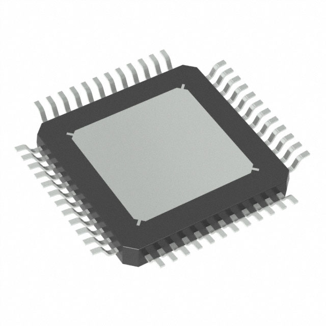
- Part No.:
- TMC6200-TA
- Manufacturer:
- Analog Devices Inc./Maxim Integrated
- Category:
- Gate Drivers
- Package:
- 48-TQFP Exposed Pad
- Datasheet:
-
 TMC6200-TA.pdf
- Description:
- IC GATE DRVR HALF-BRIDGE 48TQFP
- Quantity:
- Payment:

- Shipping:

Inventory:1,881
Please send an inquiry. Send us your inquiry, and we will respond immediately.
Product details
Overview
TMC6200-TA from TRINAMIC Motion Control GmbH & Co. KG is a high-voltage 3-phase gate driver IC for BLDC and PMSM motors, supporting external MOSFETs up to 100A coil current, operating across 8–60V DC supply, with programmable gate drive strength (0.5/1/1.5A), integrated 3-channel in-line current sense amplifiers (gain ×5/×10), and SPI + standalone dual-mode control - deployed in industrial servo drives, robotics, and CNC motion systems.
For engineers reviewing the TMC6200-TA datasheet, TMC6200-TA pinout, TMC6200-TA application, or TMC6200-TA equivalent, key selection considerations include its TQFP-EP-48 package with exposed thermal pad, BBM break-before-make logic, charge pump enabling 100% duty cycle, safe hold-off resistances (1Ω LS / 1.3Ω HS), and diagnostics via SPI including short-circuit and temperature monitoring.
Technical Context
The TMC6200-TA implements a universal 3-half-bridge gate driver architecture with integrated high-side and low-side drivers per phase (U/V/W), each supporting independent or polarity/enable control modes. It embeds a 24MHz internal oscillator, OTP-configurable protection thresholds, and dual-path current sensing - one path using three dedicated analog inputs (USENSE/VSENSE/WSENSE) feeding programmable gain amplifiers, the other supporting single-shunt configurations via internal multiplexing.
Its power architecture includes a charge pump (VCP) for high-side gate bias, an internal 11.5V regulator (12VOUT) for low-side drivers, and a 5V regulator (5VOUT) for digital logic - all supplied from VSA, which may be tied to VS or driven externally to reduce thermal load at high VM. The DRV_EN and SPE pins enable hardware-level mode selection and fault recovery.
Key Specifications
| Parameter | Value and Actual Design Meaning |
|---|---|
| Supply Voltage Range | 8–60V DC on VS pin - supports 12V/24V/48V motor bus systems with overvoltage protection design margin. |
| Max Motor Current | Up to 100A coil current - enabled by external MOSFET selection and thermal management of PCB layout. |
| Gate Drive Strength | Programmable 0.5A / 1A / 1.5A - configurable via IDRV[1:0] pins or SPI register to match MOSFET gate charge (QG) and switching speed requirements. |
| Current Sense Gain | ×5 or ×10 (standalone), ×20 (SPI-only) - sets output swing range for ADC interfacing; ×20 requires SPI mode activation. |
| Protection Features | Programmable short-circuit detection, overtemperature shutdown, and fault reporting via FAULT pin - enables fail-safe torque-off in safety-critical motion systems. |
| Control Interface | SPI (40-bit command/status) or pin-strapped standalone mode - allows trade-off between diagnostic depth and BOM simplicity. |
| Package Thermal Design | TQFP-EP-48 (7×7mm² body, 9×9mm² with leads) with exposed die pad - requires ≥6 thermal vias to internal GND plane for ≤3.5°C/W junction-to-board thermal resistance. |
Pinout & Package
TMC6200-TA is housed in a thermally enhanced TQFP-EP-48 package (7×7mm² body, 9×9mm² with leads), featuring an exposed die pad soldered directly to a solid GND plane for optimal heat dissipation and low-inductance return paths. Pin pitch is 0.5mm; double pin spacing isolates high-voltage domains (VS, U/V/W, HS/LS outputs) from low-voltage logic (VCC_IO, SPI, sense outputs).
| Pin/Terminal | Circuit Role | Design Meaning |
|---|---|---|
| UH, VH, WH | High-side gate driver outputs | Drive gates of upper MOSFETs in U/V/W half-bridges; require bootstrap capacitors (CU/CV/CW) referenced to respective phase terminals. |
| LSU, LSV, LSW | Low-side gate driver outputs | Directly drive lower MOSFET gates; powered from 12VOUT regulator - must be decoupled with ≥2.2µF ceramic capacitor near pin. |
| USENSE, VSENSE, WSENSE | Analog current sense inputs | Connect to motor-side of shunt resistors; protected by 10–22Ω series resistors; feed internal programmable-gain amplifiers (CURU/CURV/CURW outputs). |
| CSN_IDRV0, SCK_IDRV1, SDI_AMPLx10, SDO_SINGLE | Dual-function interface pins | In SPI mode (SPE=1): standard SPI signals; in standalone mode (SPE=0): configure gate drive strength and sense gain via pull-up/down. |
| DRV_EN | Positive-active enable input | Drives all gate outputs to high-impedance state when low; required to clear FAULT condition after error event. |
| FAULT | Open-drain diagnostic output | Asserts high during overtemperature, short-circuit, or undervoltage lockout; cleared only by toggling DRV_EN. |
Key Features
| Feature | Design Value |
|---|---|
| Charge pump for 100% duty cycle | Enables continuous high-side conduction without bootstrap capacitor recharge limitations - critical for servo holding and regenerative braking. |
| BBM break-before-make logic | Hardware-enforced dead-time prevents shoot-through during commutation - configurable via pin or SPI for single/dual-line control schemes. |
| 3 floating sense amplifiers | Independent ×5/×10 gain per phase supports FOC current loop accuracy down to ±0.5% full-scale with matched shunts and proper PCB layout. |
| Safe hold-off gate resistances | 1Ω (LS) and 1.3Ω (HS) internal off-state resistors minimize Miller-induced cross-conduction risk during fast dV/dt transients. |
| OTP memory programming | Allows factory pre-configuration of BBM time, short-detection sensitivity, and temperature thresholds - eliminates runtime SPI writes in cost-sensitive applications. |
Applications
| Industrial Servo Drives | Collaborative Robotics |
|---|---|
|
Use Scenario: High-bandwidth position control of PMSM servos in packaging machinery with real-time torque feedback and thermal derating. IC Role / Device Role / Timing Role: Gate driver for 3-phase inverter stage; interfaces with TMC4671 FOC controller via SPI for closed-loop current regulation and diagnostics. Use Value: Integrated current sensing eliminates external op-amps and reduces signal path noise - enabling <10µs current loop latency and ±0.2% torque linearity. |
Use Scenario: Compact, torque-limited joint actuation in cobots requiring safe current limiting and rapid fault response under dynamic load changes. IC Role / Device Role / Timing Role: High-voltage gate driver with programmable short-circuit threshold and FAULT pin assertion within 2µs of overcurrent event. Use Value: Safe hold-off resistances and BBM logic prevent destructive shoot-through during emergency stop - meeting ISO/TS 15066 power-limiting requirements. |
| CNC Spindle Control | Automated Surveillance Cameras |
|
Use Scenario: Variable-speed spindle drive for milling machines operating from 24V to 48V bus with wide RPM range and smooth acceleration profiles. IC Role / Device Role / Timing Role: 3-half-bridge driver supporting both trapezoidal BLDC and sinusoidal FOC commutation; configured via SPI for adaptive current gain and thermal monitoring. Use Value: Programmable gate drive strength (0.5–1.5A) matches diverse MOSFET QG values - enabling optimized EMI performance across 1kW–3kW spindle power levels. |
Use Scenario: Pan-tilt-zoom (PTZ) mechanism with silent, jitter-free motion and low standby power consumption in battery-backed IP cameras. IC Role / Device Role / Timing Role: Standalone-mode gate driver with zero-standby-current capability via VSA switching; uses internal 5VOUT to power microcontroller during sleep. Use Value: External VSA control enables complete power-down of gate drivers and charge pump - reducing quiescent current to <100µA while retaining fast wake-up response. |
Equivalent & Alternatives
The following parts are listed as comparable options for similar 3-phase gate driver applications.
| Alternative Part | Technical Difference | Application Difference | Selection Advice |
|---|---|---|---|
| STSPIN32F0B | Integrated 32-bit ARM Cortex-M0 MCU + gate drivers + 3-shunt current sensing; no external MOSFET support - monolithic solution. | Best for compact, low-power BLDC systems (<20A) where MCU integration reduces board area and firmware coupling is acceptable. | Select STSPIN32F0B when system-level integration outweighs flexibility; TMC6200-TA remains preferred for >50A, high-reliability industrial inverters with discrete MOSFET optimization. |
| DRV8305-Q1 | Automotive-grade 3-phase gate driver with integrated current sense amplifiers (fixed ×20 gain), but no charge pump - limited to <99% duty cycle. | Targeted at ASIL-B automotive EPS and HVAC; lacks OTP configuration and standalone pin-strapped mode of TMC6200-TA. | Choose DRV8305-Q1 only for AEC-Q100-compliant designs; TMC6200-TA offers broader voltage range (8–60V vs. 4.5–45V), higher gate drive (1.5A vs. 1A), and 100% duty cycle support. |
Compared with STSPIN32F0B and DRV8305-Q1, the TMC6200-TA delivers superior scalability for high-current industrial motors, field-proven robustness in factory automation environments, and flexible deployment across standalone and SPI-controlled architectures - making it the optimal choice for designers prioritizing thermal resilience, diagnostic depth, and long-term BOM stability.
Availability
TMC6200-TA is available at Aetrix Electronics and suitable for industrial servo drives, collaborative robotics, and CNC motion control systems requiring stable component supply, long lifecycle support, and traceable sourcing from authorized channels.
Supply support for TMC6200-TA includes scheduled delivery planning, volume procurement assistance, BOM continuity management, traceable sourcing, and lifecycle availability coordination for OEM customers, industrial embedded developers, connected-device designers, and electronics production programs.
Manufacturer
TRINAMIC Motion Control GmbH & Co. KG is a German semiconductor company specializing in high-performance motion control ICs, known for field-oriented control (FOC) algorithms, integrated drivers, and precision motor control solutions.
The TMC6200-TA belongs to TRINAMIC's high-voltage gate driver product line, designed specifically for ruggedized 3-phase motor drive stages in industrial automation, robotics, and precision machinery - emphasizing thermal resilience, diagnostic completeness, and seamless interoperability with FOC controllers like the TMC467x family.
FAQ
What is the maximum motor voltage supported by the TMC6200-TA?
The TMC6200-TA supports a motor supply voltage (VS) range of 8–60V DC, with absolute maximum rating of 65V. Operation above 48V requires careful thermal management due to increased power dissipation in the internal 11.5V gate regulator - external VSA supply is recommended for sustained 60V operation to maintain junction temperature below 125°C.
Does the TMC6200-TA support 100% duty cycle operation?
Yes, the TMC6200-TA supports true 100% duty cycle operation via its integrated charge pump circuit (VCP), which generates boosted gate voltage for high-side MOSFETs independent of bootstrap capacitor recharge timing - essential for servo holding, regenerative braking, and precise torque control in FOC applications.
How many current sense amplifiers does the TMC6200-TA integrate?
The TMC6200-TA integrates three independent, programmable-gain current sense amplifiers - one per motor phase (U/V/W) - with selectable gain of ×5 or ×10 in standalone mode, and ×20 when configured via SPI. Each amplifier accepts differential inputs from shunt resistors connected to USENSE/VSENSE/WSENSE pins.
Can the TMC6200-TA operate without an external microcontroller?
Yes, the TMC6200-TA supports fully autonomous operation in standalone mode (SPE = low), where gate drive strength, current sense gain, and BBM logic are configured via four dedicated pins (CSN, SCK, SDI, SDO). No SPI interface or firmware is required - ideal for cost-sensitive BLDC applications with fixed motor parameters.
What thermal management is required for the TMC6200-TA in high-current applications?
The TMC6200-TA requires direct thermal connection of its exposed die pad to a multi-layer PCB's internal GND plane using ≥6 thermal vias (0.3mm diameter, 0.5mm pitch). For 100A motor current, ambient temperature must be kept ≤55°C, and copper area under the IC should exceed 400mm² to achieve ≤3.5°C/W junction-to-board thermal resistance per TRINAMIC layout guidelines.
TMC6200-TA Specifications
- Product attributes
- Attribute value
- Manufacturer:
- Analog Devices Inc./Maxim Integrated
- Series:
- -
- Package/Case:
- 48-TQFP Exposed Pad
- Packaging:
- Tray
- Product Status:
- Active
- Programmable:
- Not Verified
- Driven Configuration:
- Half-Bridge
- Channel Type:
- 3-Phase
- Number of Drivers:
- 3
- Gate Type:
- N-Channel MOSFET
- Voltage - Supply:
- 10V ~ 60V
- Logic Voltage - VIL, VIH:
- -
- Current - Peak Output (Source, Sink):
- 1.5A, 1.5A
- Input Type:
- CMOS
- High Side Voltage - Max (Bootstrap):
- 85 V
- Rise / Fall Time (Typ):
- 20ns, 20ns
- Operating Temperature:
- -40°C ~ 125°C (TJ)
- Grade:
- -
- Qualification:
- -
- Mounting Type:
- Surface Mount
- Supplier Device Package:
- 48-TQFP-EP (7x7)
TMC6200-TA FAQ
1.How can I place an order for TMC6200-TA through Aetrix?
Please submit a Request for Quotation (RFQ) for TMC6200-TA on Aetrix. Our sales agent will provide a competitive quotation and guide you through the order confirmation once you accept the terms.
2.Are the price and stock information for TMC6200-TA reliable?
The price and inventory of TMC6200-TA are updated periodically and may fluctuate due to market conditions. Stock and pricing data are typically refreshed every 24 hours. Quotation validity for TMC6200-TA is usually 5 days.
3.What payment methods are accepted for TMC6200-TA?
We accept Wire Transfer, PayPal, Credit Card, Western Union, MoneyGram, and Escrow for TMC6200-TA transactions.
Note: Certain payment methods may incur a processing fee.
4.How is shipping managed for TMC6200-TA?
TMC6200-TA orders can be shipped via leading logistics carriers, including DHL, UPS, FedEx, TNT, or Registered Mail.
Once your TMC6200-TA order is processed, you will receive an email with the shipment details and tracking number.
Note: Tracking information may take up to 24 hours to appear. Express delivery typically takes 3–5 business days.
5.How can I obtain technical support or documentation for TMC6200-TA?
For technical support, including TMC6200-TA datasheets, pinout diagrams, or application guidance, please contact our engineering support team. They can provide detailed documentation and assistance for your TMC6200-TA requirements.
6.How does Aetrix verify that TMC6200-TA is sourced from the original manufacturer or authorized distributors?
All TMC6200-TA products on Aetrix are procured from qualified distributors and authorized channels. Our dedicated quality assurance team conducts strict verification, including traceability checks and, if necessary, third-party testing. This ensures that TMC6200-TA meets industry standards.
7.What is the process for return or replacement of TMC6200-TA?
All TMC6200-TA units undergo pre-shipment inspection (PSI). If there is an issue with TMC6200-TA, returns or replacements are accepted under the following conditions:
1.Quantity discrepancies, incorrect items, or visible external defects (such as breakage or corrosion), acknowledged by Aetrix.
2.The issue is reported within 90 days of delivery.
3.The TMC6200-TA part is unused and in its original packaging.
Return procedure for TMC6200-TA:
1.Submit a request within 90 days.
2.Obtain a Return Material Authorization (RMA) from Aetrix.
TMC6200-TA Tags

-
ZXGD3009E6TA
Diodes Incorporated
-
1EDN7512BXTSA1
Infineon Technologies

-
UCC27517DBVR
Texas Instruments

-
MCP1416T-E/OT
Microchip Technology
-
MCP1402T-E/OT
Microchip Technology
-
MCP1415T-E/OT
Microchip Technology
-
MCP1401T-E/OT
Microchip Technology
-
IX4428NTR
Littelfuse Inc.

-
IRS2005STRPBF
Infineon Technologies
-
IRS2008STRPBF
Infineon Technologies
-
IX4310TTR
Littelfuse Inc.

-
2EDN7524RXTMA1
Infineon Technologies
Tech Hub

A practical engineering guide to 3.3V and 5V logic compatibility, input thresholds, resistor dividers, translator ICs, MOSFET level shifting, I2C pull-ups, timing limits and power-sequencing risks.

The 74HC595 uses push-pull logic outputs, while the TPIC6B595 uses 50 V open-drain DMOS sinks for higher-power loads. This guide compares timing, current limits, 3.3 V interfacing, load wiring, thermal…

The 74HC595 converts serial data into eight stable parallel outputs. This guide covers pin functions, shift and storage timing, OE and MR behavior, drive-current limits, cascading, voltage compatibilit…

A technical comparison of level-sensitive latches and edge-triggered flip-flops, covering timing windows, setup and hold limits, master–slave operation, time borrowing, race-through, HDL inference and…

A D latch stores one bit while Enable controls when data can pass. This reference covers gate-level operation, truth tables, transparency, setup and hold timing, LE versus OE, common ICs and practical …

An SR latch stores one bit through cross-coupled feedback. This engineering reference covers NOR and NAND implementations, truth tables, forbidden-state recovery, gated operation, switch debouncing, fa…

Latch circuits retain one bit through feedback. This technical reference covers SR and D latches, truth tables, transparency, timing limits, latch-versus-flip-flop behavior, applications and common log…

An engineering guide to LED driver operation, constant-current and constant-voltage outputs, linear and switching topologies, dimming, IC selection, calculations, replacement compatibility, and fault c…

Operational amplifier guide covering op amp basics, feedback, ideal vs real op amps, common configurations, buffer circuits, offset, bias current, gain-bandwidth, slew rate, rail-to-rail limits and sel…

Jumper cables guide covering safe connection order, red and black clamp placement, final ground connection, cable gauge, length, clamp quality, copper vs CCA cables, jump starter comparison and battery…


