
 My Inquiry
 My Account


Texas Instruments TPS65910A31A1RSLT
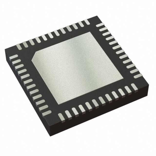
- Part No.:
- TPS65910A31A1RSLT
- Manufacturer:
- Texas Instruments
- Category:
- Power Management - Specialized
- Package:
- 48-VFQFN Exposed Pad
- Datasheet:
-
 TPS65910A31A1RSLT.pdf
- Description:
- IC PWR MGMT 4DCDC/8 LDO 48VQFN
- Quantity:
- Payment:

- Shipping:

Inventory:619
Please send an inquiry. Send us your inquiry, and we will respond immediately.
Product details
Overview
TPS65910A31A1RSLT from Texas Instruments is an integrated power-management unit (PMU) designed for OMAP- and AM335x-based systems, featuring three step-down DC-DC converters (VDD1, VDD2, VIO), one step-up 5-V converter (VDD3), eight LDOs, and a real-time clock with 32.768-kHz crystal support. It delivers dynamic voltage scaling via SmartReflex Class 3 interface and thermal shutdown protection for portable handheld and industrial applications.
For engineers reviewing the TPS65910A31A1RSLT datasheet, TPS65910A31A1RSLT pinout, TPS65910A31A1RSLT application, or TPS65910A31A1RSLT equivalent, this device supports precise power sequencing for dual-core processors, DDR memory supply management, and backup battery operation - critical for embedded Linux platforms requiring multi-rail stability and low-power sleep states.
Technical Context
The TPS65910A31A1RSLT implements an embedded power controller (EPC) to manage boot-up, sleep/wake transitions, and fault recovery sequences in OMAP/AM335x systems. Its dual SmartReflex interfaces (SR-I2C and CTL-I2C) enable independent control of VDD1/VDD2 output voltages based on processor load states, while internal 3-MHz switching synchronization minimizes EMI across all SMPS channels.
It integrates analog references (VREF, REFGND), RTC oscillator circuitry with programmable alarm, and configurable GPIO/CKSYNC for external clock injection. The device uses a single 48-pin QFN (RSL) package with exposed thermal pad and supports both crystal (32.768 kHz) and internal RC oscillator modes for timekeeping.
Key Specifications
| Parameter | Value and Actual Design Meaning |
|---|---|
| Package | 48-pin QFN (RSL), 6.0 mm × 6.0 mm, exposed thermal pad - enables high-density PCB layout and efficient heat dissipation in space-constrained handheld designs. |
| VDD1/VDD2 SMPS | Adjustable 0.5625 V to 1.5375 V (12.5-mV steps); supports dynamic voltage scaling for ARM Cortex-A8/A9 cores in AM335x SoCs. |
| VIO SMPS | Fixed 3.3 V output (±2%) at up to 1.5 A - powers I/O peripherals and memory interfaces without external feedback components. |
| VDD3 Boost Converter | 5-V output at up to 200 mA - supplies USB PHY, camera modules, or other 5-V peripherals directly from single-cell Li-ion input. |
| RTC Accuracy | ±20 ppm crystal tolerance + ±0.5 ppm/°C tempco - ensures calendar/timekeeping accuracy within ±1.5 sec/day over –40°C to 85°C. |
| I²C Interfaces | Two independent high-speed I²C buses: SR-I2C (SmartReflex Class 3) and CTL-I²C (general-purpose control) - allow concurrent voltage control and system monitoring. |
| Thermal Protection | Hot-die detection with automatic shutdown at TJ ≥ 125°C and hysteresis reset at TJ ≤ 115°C - prevents permanent damage during sustained overload conditions. |
Pinout & Package
TPS65910A31A1RSLT is housed in a 48-pin QFN (RSL) package with 0.4-mm pitch and exposed thermal pad (PowerPad). The package measures 6.0 mm × 6.0 mm × 0.8 mm and requires solder paste stencil design per JEDEC J-STD-020 for moisture sensitivity level 3.
| Pin/Terminal | Circuit Role | Design Meaning |
|---|---|---|
| VDDIO | Digital I/O supply rail | Provides 1.65–3.45 V power to all digital interface pins (I²C, GPIO, INT1); must be externally decoupled with ≥100 nF capacitor. |
| SDA_SDI / SCL_SCK | CTL-I²C bidirectional data/clock | Primary control interface for register access, LDO enable/disable, and SMPS configuration; supports 400-kHz fast-mode operation. |
| SDASR_EN2 / SCLSR_EN1 | SR-I²C bidirectional data/clock | Dedicated SmartReflex interface for real-time VDD1/VDD2 voltage adjustment by host processor - no software polling required. |
| SLEEP | Active-low sleep state control | Drives device into low-power retention mode when asserted; reduces quiescent current to <10 µA while preserving register state and RTC operation. |
| CLK32KOUT | 32.768-kHz clock output | Buffered RTC oscillator output for feeding external baseband or audio subsystems; disabled in SLEEP unless configured via register. |
| VBACKUP | Backup battery input | Accepts 1.8–5.5 V from coin cell or supercapacitor to maintain RTC and backup registers during main power loss. |
Key Features
| Feature | Design Value |
|---|---|
| Embedded Power Controller (EPC) | Hardware-managed power-on reset, boot sequencing, and fault recovery - eliminates need for external CPLD or firmware coordination in AM335x reference designs. |
| SmartReflex Class 3 Compliance | Real-time, closed-loop voltage scaling of VDD1/VDD2 using dedicated SR-I²C bus - reduces dynamic power by up to 40% during CPU idle states. |
| Triple SMPS Architecture | VDD1/VDD2 (core), VIO (I/O), and VDD3 (5-V boost) operate independently with synchronized 3-MHz switching - lowers system-level EMI and simplifies filtering. |
| Eight Programmable LDOs | VAUX1/VAUX2 (300 mA each), VDAC/VPLL (for video/PLL rails), VDIG1/VDIG2 (DDR termination), VAUX33/VMMC - fully controllable via I²C with soft-start and slew-rate control. |
| Integrated RTC with Calendar | Full BCD-encoded date/time/alarm functionality plus 32.768-kHz crystal oscillator - retains time across power cycles using VBACKUP supply without external RTC chip. |
Applications
| Industrial HMI Panel | AM335x-Based Edge Gateway |
|---|---|
Use Scenario: Fanless enclosure with ARM Cortex-A8 processor, capacitive touchscreen, and CAN/RS-485 interfaces operating in -40°C to 85°C ambient. IC Role / Device Role / Timing Role: Central PMU managing core voltage scaling, DDR2/3 termination, RTC timestamping for event logging, and 5-V USB host power. Use Value: Single-chip solution eliminates discrete LDOs and timing ICs, reducing BOM count by 12 components and enabling full-system sleep with <15 µA standby current. | Use Scenario: Secure IoT gateway with dual-band Wi-Fi, TLS acceleration, and local MQTT broker running Yocto Linux on AM335x with DDR3. IC Role / Device Role / Timing Role: Power sequencer for boot initialization, SmartReflex-controlled VDD1/VDD2 during CPU frequency transitions, and VIO-regulated 3.3-V I/O for Ethernet PHY and SDIO. Use Value: Hardware-based sequencing ensures deterministic boot within 120 ms; SR-I²C interface allows Linux cpufreq driver to adjust voltages without kernel patching. |
| Portable Medical Monitor | Automated Test Equipment (ATE) |
Use Scenario: Battery-powered vital signs monitor with OLED display, ECG front-end, and Bluetooth LE connectivity. IC Role / Device Role / Timing Role: Multi-rail regulator supplying 1.2-V core, 3.3-V analog sensors, 5-V USB charging, and RTC-backed data logging with tamper-proof timestamps. Use Value: Integrated backup battery management maintains RTC and last-measurement registers for 72+ hours after main battery depletion. | Use Scenario: Rack-mounted test instrument with FPGA-based signal generation, precision ADC/DAC, and PCIe host interface. IC Role / Device Role / Timing Role: Power supervisor for FPGA configuration voltage (1.2 V), analog reference (2.5 V), and PCIe 3.3-V auxiliary rail - coordinated via EPC state machine. Use Value: Pin-strapped BOOT0/BOOT1 selection enables field-upgradable power profiles; thermal shutdown prevents FPGA latch-up during extended burn-in tests. |
Equivalent & Alternatives
The following parts are listed as comparable options for similar power-management applications.
| Alternative Part | Technical Difference | Application Difference | Selection Advice |
|---|---|---|---|
| TPS65910A3A1RSL | Same silicon die, identical SMPS/LDO specs, but configured for AM335x with DDR2 (not DDR3) memory interface timing. | Lacks DDR3-specific power sequencing logic and VREF calibration for DDR3L termination; not validated for AM335x DDR3 designs. | Select only for legacy AM335x DDR2 platforms; incompatible with DDR3 VTT/VREF requirements. |
| TPS65217CZQZR | Single 48-QFN PMU with 3 SMPS + 7 LDOs; lacks SmartReflex Class 3 interface and RTC calendar functionality. | No hardware power sequencing engine; requires external microcontroller for boot coordination; no integrated 32.768-kHz RTC oscillator. | Use where cost-sensitive designs omit SmartReflex and RTC features; requires additional firmware and external crystal. |
Compared with TPS65910A31A1RSLT, TPS65910A3A1RSL omits DDR3-specific power sequencing and VREF calibration, while TPS65217CZQZR removes SmartReflex Class 3 and RTC calendar - making TPS65910A31A1RSLT uniquely suited for AM335x DDR3 Linux platforms needing autonomous power control and time-stamped data logging.
Availability
TPS65910A31A1RSLT is available at Aetrix Electronics and suitable for industrial HMI panels, AM335x-based edge gateways, and portable medical monitors requiring stable component supply, long-term lifecycle support, and guaranteed traceability for ISO 13485 and IEC 62304 compliance.
Supply support for TPS65910A31A1RSLT includes scheduled delivery planning, volume procurement assistance, BOM continuity management, traceable sourcing, and lifecycle availability coordination for OEM customers, industrial embedded developers, connected-device designers, and electronics production programs.
Manufacturer
Texas Instruments is a global semiconductor leader delivering analog, embedded processing, and connectivity solutions for industrial, automotive, and consumer markets.
The TPS65910 family is engineered specifically for OMAP- and Sitara™-based application processors, providing tightly integrated power sequencing, SmartReflex voltage scaling, and RTC functionality to simplify system-level power architecture in Linux-capable embedded platforms.
FAQ
What is the primary application target for the TPS65910A31A1RSLT?
The TPS65910A31A1RSLT is specifically designed for AM335x-based systems with DDR3 memory, such as industrial gateways and embedded Linux platforms. It provides hardware-coordinated power sequencing, SmartReflex Class 3 voltage scaling for dual-core operation, and integrated RTC with calendar - all validated for TI's AM335x DDR3 reference designs per SWCU093 documentation.
Does the TPS65910A31A1RSLT support external 32.768-kHz crystal operation?
Yes, the TPS65910A31A1RSLT supports external 32.768-kHz crystal operation via OSC32KIN/OSC32KOUT pins with load capacitance range of 6–12.5 pF. It also includes an internal RC oscillator as fallback. Crystal accuracy is specified at ±20 ppm at 27°C, with temperature coefficient of ±0.5 ppm/°C - ensuring reliable RTC operation across –40°C to 85°C.
How does the SmartReflex Class 3 interface function on the TPS65910A31A1RSLT?
The TPS65910A31A1RSLT implements two dedicated I²C lines (SDASR_EN2/SCLSR_EN1) for SmartReflex Class 3 communication. This interface allows the host processor to dynamically adjust VDD1 and VDD2 output voltages in real time based on workload, without CPU intervention or register polling - reducing dynamic power consumption by up to 40% during low-load states.
What thermal protection mechanisms are built into the TPS65910A31A1RSLT?
The TPS65910A31A1RSLT includes thermal shutdown protection that triggers at junction temperature ≥125°C and resets automatically when temperature falls to ≤115°C. It also features hot-die detection with interrupt assertion on INT1 pin, enabling host firmware to initiate cooling or throttling before shutdown occurs - critical for fanless industrial enclosures.
Can the TPS65910A31A1RSLT operate from a single-cell Li-ion battery?
Yes, the TPS65910A31A1RSLT is explicitly designed for single-cell Li-ion (2.7–5.5 V) or 3-cell Ni-MH input. All SMPS inputs (VCC1, VCC2, VCCIO, etc.) accept 2.7–5.5 V, and the VDD3 boost converter generates regulated 5 V from as low as 2.7 V input - enabling full functionality across the entire Li-ion discharge curve without external pre-regulation.
TPS65910A31A1RSLT Specifications
- Product attributes
- Attribute value
- Manufacturer:
- Texas Instruments
- Series:
- -
- Package/Case:
- 48-VFQFN Exposed Pad
- Packaging:
- Tape & Reel (TR)
- Product Status:
- Active
- Applications:
- Handheld/Mobile Devices, OMAP™
- Current - Supply:
- -
- Voltage - Supply:
- 1.7V ~ 5.5V
- Operating Temperature:
- -40°C ~ 85°C
- Grade:
- -
- Qualification:
- -
- Mounting Type:
- Surface Mount
- Supplier Device Package:
- 48-VQFN (6x6)
TPS65910A31A1RSLT FAQ
1.How can I place an order for TPS65910A31A1RSLT through Aetrix?
Please submit a Request for Quotation (RFQ) for TPS65910A31A1RSLT on Aetrix. Our sales agent will provide a competitive quotation and guide you through the order confirmation once you accept the terms.
2.Are the price and stock information for TPS65910A31A1RSLT reliable?
The price and inventory of TPS65910A31A1RSLT are updated periodically and may fluctuate due to market conditions. Stock and pricing data are typically refreshed every 24 hours. Quotation validity for TPS65910A31A1RSLT is usually 5 days.
3.What payment methods are accepted for TPS65910A31A1RSLT?
We accept Wire Transfer, PayPal, Credit Card, Western Union, MoneyGram, and Escrow for TPS65910A31A1RSLT transactions.
Note: Certain payment methods may incur a processing fee.
4.How is shipping managed for TPS65910A31A1RSLT?
TPS65910A31A1RSLT orders can be shipped via leading logistics carriers, including DHL, UPS, FedEx, TNT, or Registered Mail.
Once your TPS65910A31A1RSLT order is processed, you will receive an email with the shipment details and tracking number.
Note: Tracking information may take up to 24 hours to appear. Express delivery typically takes 3–5 business days.
5.How can I obtain technical support or documentation for TPS65910A31A1RSLT?
For technical support, including TPS65910A31A1RSLT datasheets, pinout diagrams, or application guidance, please contact our engineering support team. They can provide detailed documentation and assistance for your TPS65910A31A1RSLT requirements.
6.How does Aetrix verify that TPS65910A31A1RSLT is sourced from the original manufacturer or authorized distributors?
All TPS65910A31A1RSLT products on Aetrix are procured from qualified distributors and authorized channels. Our dedicated quality assurance team conducts strict verification, including traceability checks and, if necessary, third-party testing. This ensures that TPS65910A31A1RSLT meets industry standards.
7.What is the process for return or replacement of TPS65910A31A1RSLT?
All TPS65910A31A1RSLT units undergo pre-shipment inspection (PSI). If there is an issue with TPS65910A31A1RSLT, returns or replacements are accepted under the following conditions:
1.Quantity discrepancies, incorrect items, or visible external defects (such as breakage or corrosion), acknowledged by Aetrix.
2.The issue is reported within 90 days of delivery.
3.The TPS65910A31A1RSLT part is unused and in its original packaging.
Return procedure for TPS65910A31A1RSLT:
1.Submit a request within 90 days.
2.Obtain a Return Material Authorization (RMA) from Aetrix.
TPS65910A31A1RSLT Tags

-
TPS2511DGNR
Texas Instruments

-
UTC2000/MG
Microchip Technology

-
TUSB320HAIRWBR
Texas Instruments

-
TPS61252DSGR
Texas Instruments

-
PI5USB30216CXUAEX
Diodes Incorporated

-
SN6501DBVR
Texas Instruments

-
CYPD3177-24LQXQT
Infineon Technologies
-
SN6501QDBVRQ1
Texas Instruments

-
STUSB1600AQTR
STMicroelectronics

-
SN6505BDBVR
Texas Instruments
-
SN6501DBVT
Texas Instruments

-
TPS65150PWPR
Texas Instruments
Tech Hub

A practical engineering guide to 3.3V and 5V logic compatibility, input thresholds, resistor dividers, translator ICs, MOSFET level shifting, I2C pull-ups, timing limits and power-sequencing risks.

The 74HC595 uses push-pull logic outputs, while the TPIC6B595 uses 50 V open-drain DMOS sinks for higher-power loads. This guide compares timing, current limits, 3.3 V interfacing, load wiring, thermal…

The 74HC595 converts serial data into eight stable parallel outputs. This guide covers pin functions, shift and storage timing, OE and MR behavior, drive-current limits, cascading, voltage compatibilit…

A technical comparison of level-sensitive latches and edge-triggered flip-flops, covering timing windows, setup and hold limits, master–slave operation, time borrowing, race-through, HDL inference and…

A D latch stores one bit while Enable controls when data can pass. This reference covers gate-level operation, truth tables, transparency, setup and hold timing, LE versus OE, common ICs and practical …

An SR latch stores one bit through cross-coupled feedback. This engineering reference covers NOR and NAND implementations, truth tables, forbidden-state recovery, gated operation, switch debouncing, fa…

Latch circuits retain one bit through feedback. This technical reference covers SR and D latches, truth tables, transparency, timing limits, latch-versus-flip-flop behavior, applications and common log…

An engineering guide to LED driver operation, constant-current and constant-voltage outputs, linear and switching topologies, dimming, IC selection, calculations, replacement compatibility, and fault c…

Operational amplifier guide covering op amp basics, feedback, ideal vs real op amps, common configurations, buffer circuits, offset, bias current, gain-bandwidth, slew rate, rail-to-rail limits and sel…

Jumper cables guide covering safe connection order, red and black clamp placement, final ground connection, cable gauge, length, clamp quality, copper vs CCA cables, jump starter comparison and battery…


