
 My Inquiry
 My Account


Texas Instruments TPS65911AA2NMAT
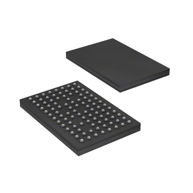
- Part No.:
- TPS65911AA2NMAT
- Manufacturer:
- Texas Instruments
- Category:
- Power Management - Specialized
- Package:
- 98-VFBGA
- Datasheet:
-
 TPS65911AA2NMAT.pdf
- Description:
- INTEGRATED POWER MANAGEMENT IC (
- Quantity:
- Payment:

- Shipping:

Inventory:177
Please send an inquiry. Send us your inquiry, and we will respond immediately.
Product details
Overview
TPS65911AA2NMAT from Texas Instruments is an integrated power management IC (PMIC) featuring three step-down DC-DC converters (VDD1, VDD2, VIO), one external-FET controller (VDDCtrl), eight programmable LDOs, embedded power controller with EEPROM, real-time clock (RTC), and nine configurable GPIOs. It delivers 1.5 A at 0.6–1.5 V on VDD1, 1.5 A at 0.6–2.2 V on VDD2, and 1.3 A at 1.5 V on VIO - optimized for dual-core processor power sequencing in portable systems.
For engineers reviewing the TPS65911AA2NMAT datasheet, TPS65911AA2NMAT pinout, TPS65911AA2NMAT application, or TPS65911AA2NMAT equivalent, this device supports dynamic voltage scaling via dedicated I²C, thermal shutdown, 32.768-kHz RTC crystal interface, and programmable power-up sequences - critical for Li-ion-powered handheld SoC platforms requiring tight rail coordination and low-power state management.
Technical Context
The TPS65911AA2NMAT implements a hierarchical power architecture: two core SMPS (VDD1/VDD2) support adaptive voltage scaling under I²C control, while VIO supplies I/O and memory rails. The VDDCtrl controller drives external high-current FETs with adjustable slew rate (5 mV/µs) and overcurrent protection via TRIP pin.
Its embedded power controller (EPC) executes EEPROM-programmable sequencing, including cold reset (HDRST), power initialization (PWRDN), and SLEEP/ACTIVE transitions. The RTC subsystem includes oscillator input/output (OSC32KIN/OSC32KOUT), calendar/alarm functions, and VRTC LDO (300 mA, 1.0–3.3 V) backed by VBACKUP input.
Key Specifications
| Parameter | Value and Actual Design Meaning |
|---|---|
| VDD1 SMPS Output | 0.6–1.5 V, 1.5 A max - powers primary processor core with DVS support |
| VDD2 SMPS Output | 0.6–2.2 V, 1.5 A max - powers secondary processor core with independent DVS |
| VIO SMPS Output | 1.5 V @ 1.3 A, 1.8 V @ 1.2 A, 2.5/3.3 V @ 1.1 A - supplies I/O and memory interfaces |
| LDO Count & Range | Eight user-programmable LDOs: five at 1–3.3 V (100-mV steps), three at 1–3.3 V (50-mV steps) |
| I²C Interface | High-speed CTL-I²C (up to 400 kHz) + optional EN1/EN2-dedicated I²C for VDD1/VDD2 scaling |
| RTC Accuracy | 32.768-kHz crystal oscillator support with ±20 ppm typical stability over –40°C to 85°C |
| Package | 98-pin BGA MicroStar Junior™, 9.0 mm × 6.0 mm, 0.65-mm pitch - requires controlled-impedance PCB layout |
Pinout & Package
TPS65911AA2NMAT is housed in a 98-ball BGA MicroStar Junior™ package (ZRC suffix), 9.0 mm × 6.0 mm body size, 0.65-mm ball pitch. Thermal pad exposed on bottom for enhanced heat dissipation; requires solder mask defined pads and stencil-applied solder paste per TI SLOA122 guidelines.
| Pin/Terminal | Circuit Role | Design Meaning |
|---|---|---|
| VDD1, VDD2, VIO | SMPS output rails | Core and I/O power outputs - each with dedicated feedback (VFB1/VFB2/VFBIO) and ground (GND1/GND2/GNDIO) |
| VDDCtrl (DRVH/DRVL/SW/VOUT) | External FET controller | Drives high-side NMOS (DRVH) and low-side NMOS (DRVL); SW node connects to external inductor; VOUT feeds feedback loop |
| EN1 / EN2 | Dual-function digital I/O | Configurable as enable signals for power resources OR dedicated I²C clock/data lines for VDD1/VDD2 voltage scaling |
| OSC32KIN / OSC32KOUT | RTC crystal interface | Supports 32.768-kHz tuning fork crystal; internal load capacitors configurable via EEPROM; enables autonomous RTC operation during sleep |
| GPIO0–GPIO8 | Configurable general-purpose I/O | Nine pins with multiplexed roles: four support enable sequencing, two drive LEDs (10-mA sink), two support clock sync, all generate maskable interrupts |
Key Features
| Feature | Design Value |
|---|---|
| EEPROM-programmable power sequencing | Enables custom boot-up/shutdown order across all 12 power rails without firmware changes |
| Dedicated VDD1/VDD2 DVS I²C interface | Reduces latency and bus contention versus shared CTL-I²C - critical for real-time DVFS in ARM Cortex-A9/A15 systems |
| Integrated RTC with backup battery input (VBACKUP) | Maintains time/calendar during main power loss; supports coin-cell or supercapacitor backup without external circuitry |
| Thermal monitoring with hot-die detection | Triggers automatic shutdown at 125°C junction temperature; provides NRESPWRON signal for system-level thermal response |
| Programmable LED/PWM generators | Two ON/OFF pulse generators + one PWM generator - drive status LEDs directly without MCU intervention |
| Comparator inputs (VCCS) | Two analog comparators referenced to internal bandgap (VREF) - enable custom voltage monitoring or system event triggering |
Applications
| Smartphone Application Processor Power | Tablet SoC Power Management |
|---|---|
|
Use Scenario: Powers NVIDIA T30 dual-core Cortex-A9 application processor with DDR2/DDR3 memory interface. IC Role / Device Role / Timing Role: PMIC provides sequenced VDD1/VDD2 cores, VIO for DDR I/O, LDOs for peripherals, and RTC for suspend/resume timing. Use Value: Enables full DVS across both cores using dedicated I²C channels, reducing active power by up to 35% versus fixed-voltage solutions. |
Use Scenario: Manages power for TI AM3894/AM3892 DaVinci processors in industrial tablets with extended temperature requirements. IC Role / Device Role / Timing Role: Coordinates cold-start sequence, monitors thermal events via PWRDN input, and maintains RTC accuracy during battery-only operation. Use Value: Eliminates need for discrete supervisors and RTC ICs - reduces BOM count by 4 components and PCB area by 28 mm². |
| Automotive Infotainment Head Unit | Portable Medical Imaging Device |
|
Use Scenario: Supplies TI DM8168 processor in automotive infotainment system with CAN/FlexRay connectivity and display drivers. IC Role / Device Role / Timing Role: Delivers clean, low-noise VIO for display interface; uses GPIOs to control backlight dimming and audio codec enable. Use Value: Achieves <10 mVpp ripple on VIO rail at 1.8 V/1.2 A - meets CISPR-25 Class 5 EMI requirements for automotive electronics. |
Use Scenario: Powers FPGA-based ultrasound beamformer in handheld diagnostic equipment with strict low-power sleep modes. IC Role / Device Role / Timing Role: Enters ultra-low-power SLEEP state with RTC running on VBACKUP; wakes system via GPIO interrupt on sensor trigger. Use Value: Reduces standby current to 12 µA (typical) - extends battery life to >72 hours between charges in clinical use. |
Equivalent & Alternatives
The following parts are listed as comparable options for similar PMIC applications.
| Alternative Part | Technical Difference | Application Difference | Selection Advice |
|---|---|---|---|
| TPS659121AA2NMAT | Same pinout, identical feature set, but supports DDR3L memory interface and targets 66AK2G12 processor | Designed for KeyStone II multicore DSPs; lacks DDR2 support present in TPS65911AA2NMAT | Select when targeting TI 66AK2Gxx SoCs and requiring DDR3L compatibility |
| TPS6591133AA2NMAT | Identical electrical specs and pinout; differs only in EEPROM configuration and supported processor list (DM814x series) | Optimized for TI DaVinci DM8148/DM8147 processors; same thermal and sequencing capabilities | Choose for legacy DaVinci-based designs where TPS65911AA2NMAT EEPROM settings are not validated |
Compared with TPS65911AA2NMAT, TPS659121AA2NMAT adds DDR3L support for newer TI DSPs, while TPS6591133AA2NMAT offers identical hardware with preconfigured sequencing for DaVinci DM814x - both require no PCB changes but differ in factory-programmed EEPROM content and target processor alignment.
Availability
TPS65911AA2NMAT is available at Aetrix Electronics and suitable for smartphone application processor power, tablet SoC power management, automotive infotainment head units, and portable medical imaging devices requiring stable component supply across multi-year production cycles.
Supply support for TPS65911AA2NMAT includes scheduled delivery planning, volume procurement assistance, BOM continuity management, traceable sourcing, and lifecycle availability coordination for OEM customers, industrial embedded developers, connected-device designers, and electronics production programs.
Manufacturer
Texas Instruments is a global semiconductor leader specializing in analog, embedded processing, and power management technologies, with over 50 years of innovation in energy-efficient IC design.
The TPS65911 product line was engineered specifically for single-chip power management of heterogeneous multicore processors in portable and handheld systems - integrating sequencing, regulation, RTC, and GPIOs to replace 6+ discrete components.
FAQ
What is the maximum output current capability of the VDD1 SMPS in the TPS65911AA2NMAT?
The TPS65911AA2NMAT VDD1 SMPS delivers up to 1.5 A continuous output current across its 0.6 V to 1.5 V adjustable range. This rating is validated at 85°C ambient with proper PCB thermal design and applies to both steady-state and transient loads per Section 5.14 of the datasheet. The TPS65911AA2NMAT includes overcurrent protection that limits peak current to prevent damage during short-circuit events.
Does the TPS65911AA2NMAT support external 32.768-kHz crystal oscillators for RTC operation?
Yes, the TPS65911AA2NMAT supports external 32.768-kHz crystal oscillators via dedicated OSC32KIN and OSC32KOUT pins. Internal load capacitance is configurable through EEPROM registers, eliminating the need for external capacitors in most designs. The TPS65911AA2NMAT also includes a 32-kHz RC oscillator as a backup when crystal is unavailable or fails.
How many LDO regulators does the TPS65911AA2NMAT integrate, and what are their key specifications?
The TPS65911AA2NMAT integrates eight fully programmable LDO regulators: LDO1/LDO2 (320 mA, 1.0–3.3 V, 50-mV steps), LDO3/LDO4 (200/50 mA, 1.0–3.3 V, 100-mV steps), LDO5–LDO8 (300 mA each, 1.0–3.3 V, 100-mV steps). All are digitally controlled via I²C and support soft-start, current limiting, and thermal foldback - confirmed in Sections 5.17–5.20 of the TPS65911AA2NMAT datasheet.
Can the EN1 and EN2 pins of the TPS65911AA2NMAT be used simultaneously for power enable and I²C communication?
No - EN1 and EN2 are multiplexed pins: they operate either as general-purpose enable signals for power resources or as dedicated I²C clock/data lines for VDD1/VDD2 dynamic voltage scaling, but not both simultaneously. Configuration is determined at power-up via BOOT1 pin state and EEPROM settings. The TPS65911AA2NMAT datasheet explicitly prohibits concurrent use in Section 1.1 and Figure 1-1.
What thermal protection features are implemented in the TPS65911AA2NMAT?
The TPS65911AA2NMAT includes thermal shutdown protection that disables all SMPS and LDOs when junction temperature exceeds 125°C, plus hot-die detection that asserts NRESPWRON to signal thermal fault to the host processor. It also monitors die temperature continuously and reports status via I²C register bits - all verified in Section 5.9 and Section 6.13 of the official TPS65911AA2NMAT datasheet.
TPS65911AA2NMAT Specifications
- Product attributes
- Attribute value
- Manufacturer:
- Texas Instruments
- Series:
- -
- Package/Case:
- 98-VFBGA
- Packaging:
- Tape & Reel (TR)
- Product Status:
- Active
- Applications:
- Portable Equipment
- Current - Supply:
- 320µA
- Voltage - Supply:
- 1.7V, 2.7V ~ 5.5V
- Operating Temperature:
- -40°C ~ 85°C (TA)
- Grade:
- -
- Qualification:
- -
- Mounting Type:
- Surface Mount
- Supplier Device Package:
- 98-NFBGA (9x6)
TPS65911AA2NMAT FAQ
1.How can I place an order for TPS65911AA2NMAT through Aetrix?
Please submit a Request for Quotation (RFQ) for TPS65911AA2NMAT on Aetrix. Our sales agent will provide a competitive quotation and guide you through the order confirmation once you accept the terms.
2.Are the price and stock information for TPS65911AA2NMAT reliable?
The price and inventory of TPS65911AA2NMAT are updated periodically and may fluctuate due to market conditions. Stock and pricing data are typically refreshed every 24 hours. Quotation validity for TPS65911AA2NMAT is usually 5 days.
3.What payment methods are accepted for TPS65911AA2NMAT?
We accept Wire Transfer, PayPal, Credit Card, Western Union, MoneyGram, and Escrow for TPS65911AA2NMAT transactions.
Note: Certain payment methods may incur a processing fee.
4.How is shipping managed for TPS65911AA2NMAT?
TPS65911AA2NMAT orders can be shipped via leading logistics carriers, including DHL, UPS, FedEx, TNT, or Registered Mail.
Once your TPS65911AA2NMAT order is processed, you will receive an email with the shipment details and tracking number.
Note: Tracking information may take up to 24 hours to appear. Express delivery typically takes 3–5 business days.
5.How can I obtain technical support or documentation for TPS65911AA2NMAT?
For technical support, including TPS65911AA2NMAT datasheets, pinout diagrams, or application guidance, please contact our engineering support team. They can provide detailed documentation and assistance for your TPS65911AA2NMAT requirements.
6.How does Aetrix verify that TPS65911AA2NMAT is sourced from the original manufacturer or authorized distributors?
All TPS65911AA2NMAT products on Aetrix are procured from qualified distributors and authorized channels. Our dedicated quality assurance team conducts strict verification, including traceability checks and, if necessary, third-party testing. This ensures that TPS65911AA2NMAT meets industry standards.
7.What is the process for return or replacement of TPS65911AA2NMAT?
All TPS65911AA2NMAT units undergo pre-shipment inspection (PSI). If there is an issue with TPS65911AA2NMAT, returns or replacements are accepted under the following conditions:
1.Quantity discrepancies, incorrect items, or visible external defects (such as breakage or corrosion), acknowledged by Aetrix.
2.The issue is reported within 90 days of delivery.
3.The TPS65911AA2NMAT part is unused and in its original packaging.
Return procedure for TPS65911AA2NMAT:
1.Submit a request within 90 days.
2.Obtain a Return Material Authorization (RMA) from Aetrix.
TPS65911AA2NMAT Tags

-
TPS2511DGNR
Texas Instruments

-
UTC2000/MG
Microchip Technology

-
TUSB320HAIRWBR
Texas Instruments

-
TPS61252DSGR
Texas Instruments

-
PI5USB30216CXUAEX
Diodes Incorporated

-
SN6501DBVR
Texas Instruments

-
CYPD3177-24LQXQT
Infineon Technologies
-
SN6501QDBVRQ1
Texas Instruments

-
STUSB1600AQTR
STMicroelectronics

-
SN6505BDBVR
Texas Instruments
-
SN6501DBVT
Texas Instruments

-
TPS65150PWPR
Texas Instruments
Tech Hub

A practical engineering guide to 3.3V and 5V logic compatibility, input thresholds, resistor dividers, translator ICs, MOSFET level shifting, I2C pull-ups, timing limits and power-sequencing risks.

The 74HC595 uses push-pull logic outputs, while the TPIC6B595 uses 50 V open-drain DMOS sinks for higher-power loads. This guide compares timing, current limits, 3.3 V interfacing, load wiring, thermal…

The 74HC595 converts serial data into eight stable parallel outputs. This guide covers pin functions, shift and storage timing, OE and MR behavior, drive-current limits, cascading, voltage compatibilit…

A technical comparison of level-sensitive latches and edge-triggered flip-flops, covering timing windows, setup and hold limits, master–slave operation, time borrowing, race-through, HDL inference and…

A D latch stores one bit while Enable controls when data can pass. This reference covers gate-level operation, truth tables, transparency, setup and hold timing, LE versus OE, common ICs and practical …

An SR latch stores one bit through cross-coupled feedback. This engineering reference covers NOR and NAND implementations, truth tables, forbidden-state recovery, gated operation, switch debouncing, fa…

Latch circuits retain one bit through feedback. This technical reference covers SR and D latches, truth tables, transparency, timing limits, latch-versus-flip-flop behavior, applications and common log…

An engineering guide to LED driver operation, constant-current and constant-voltage outputs, linear and switching topologies, dimming, IC selection, calculations, replacement compatibility, and fault c…

Operational amplifier guide covering op amp basics, feedback, ideal vs real op amps, common configurations, buffer circuits, offset, bias current, gain-bandwidth, slew rate, rail-to-rail limits and sel…

Jumper cables guide covering safe connection order, red and black clamp placement, final ground connection, cable gauge, length, clamp quality, copper vs CCA cables, jump starter comparison and battery…


