
 My Inquiry
 My Account


STMicroelectronics TS419IST
- Part No.:
- TS419IST
- Manufacturer:
- STMicroelectronics
- Category:
- Audio Amplifiers
- Package:
- 8-TSSOP, 8-MSOP (0.118", 3.00mm Width)
- Datasheet:
-
 TS419IST.pdf
- Description:
- IC AMP AB MONO 367MW 8MINISO
- Quantity:
- Payment:

- Shipping:

Inventory:3,783
Please send an inquiry. Send us your inquiry, and we will respond immediately.
Product details
Overview
TS419IST from STMicroelectronics is a monaural Class AB audio power amplifier in MiniSO8 package, operating from 2 V to 5.5 V supply and delivering up to 367 mW into 16 Ω at 10% THD+N (5 V), with 95 dB A-weighted SNR and 56 dB PSRR at 1 kHz. It drives earpiece/receiver speakers in BTL mode-eliminating output coupling capacitors-and features active-high standby control, ON/OFF click suppression, and thermal protection. Used in mobile handsets and portable audio interfaces requiring low-voltage operation and capacitor-free output.
For engineers reviewing the TS419IST datasheet, TS419IST pinout, TS419IST application, or TS419IST equivalent, this page delivers verified electrical specs (e.g., 2.5 mA max ICC, 10 nA standby current), package-validated pin functions, real-world use cases in analog/digital phones and PDAs, and confirmed alternatives for earpiece driver replacement.
Technical Context
The TS419IST operates in bridge-tied-load (BTL) configuration, enabling capacitor-less 16–32 Ω speaker drive with differential output swing up to ±VCC/2. Its gain is externally set via RIN/RFEED resistors (AV = 2 × RFEED/RIN), supporting flexible system-level signal conditioning.
It integrates short-circuit limiting, thermal shutdown, and an active-high standby input that reduces quiescent current to 10 nA typical. The amplifier maintains ≥58° phase margin and 18 dB gain margin across 16 Ω loads with 400 pF capacitive loading, ensuring stable operation without external compensation.
Key Specifications
| Parameter | Value and Actual Design Meaning |
|---|---|
| Supply Voltage Range | 2 V to 5.5 V - supports single-cell Li-ion, NiMH, and 3.3 V/5 V system rails without level-shifting. |
| Output Power (16 Ω) | 367 mW @ 5 V / 10% THD+N - sufficient for high-SPL earpiece audio in compact handhelds. |
| THD+N | 0.15% typ. @ 220 mW, 16 Ω - ensures clean voice reproduction in telephony bandwidth (20 Hz–20 kHz). |
| SNR (A-weighted) | 95 dB @ 5 V - minimizes audible background noise in quiet listening environments. |
| PSRR | 56 dB typ. @ 1 kHz - rejects ripple from noisy DC-DC converters powering baseband processors. |
| Standby Current | 10 nA typ. - enables multi-week battery life in always-on receiver mode of cordless phones. |
| Slew Rate | 0.4 V/µs - prevents slew-induced distortion on transient-rich speech signals. |
Pinout & Package
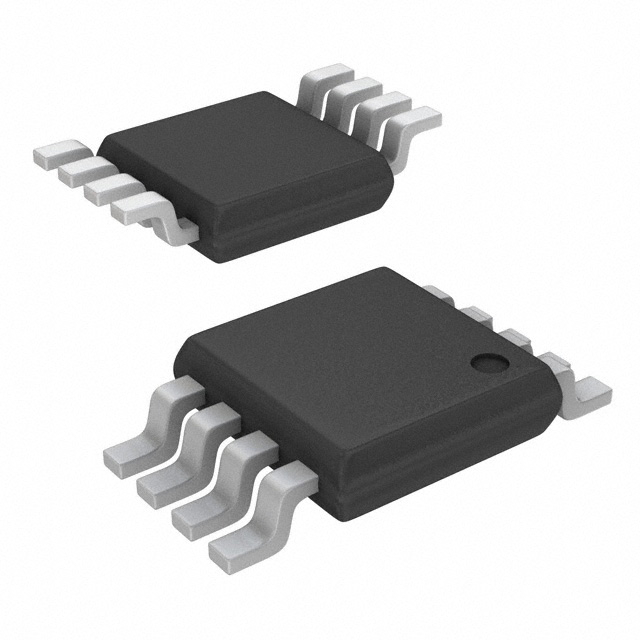
TS419IST uses the MiniSO8 (SOIC-8) surface-mount package with standard 1.27 mm pitch and exposed pad for thermal dissipation (RthJA = 190 °C/W on 4-layer PCB). Pin numbering follows JEDEC MS-012AA outline.
| Pin/Terminal | Circuit Role | Design Meaning |
|---|---|---|
| 1 - STANDBY | Active-high enable input | Drives amplifier into ultra-low-power state (10 nA) when logic low; requires pull-up for default-on operation. |
| 2 - BYPASS | Half-supply bias reference | Connects to 1 µF capacitor to GND to stabilize internal virtual ground for BTL output stage. |
| 3 - V+ | Positive supply rail | Accepts 2–5.5 V; must be decoupled with ≥1 µF ceramic capacitor near pin. |
| 4 - IN− | Inverting input | Forms feedback network with RFEED; sets closed-loop gain together with RIN. |
| 5 - VOUT2 | BTL output channel 2 | Delivers inverted audio signal; paired with VOUT1 to generate differential swing across load. |
| 6 - GND | Analog/digital ground | Single-point return for supply, inputs, and bypass cap; must connect to low-impedance PCB ground plane. |
| 7 - VCC | Power supply input | Same as V+; labeled separately for clarity but electrically identical (pin 3 and 7 tied internally). |
| 8 - VOUT1 | BTL output channel 1 | Delivers non-inverted audio signal; differential voltage between VOUT1 and VOUT2 drives speaker directly. |
Key Features
| Feature | Design Value |
|---|---|
| Capacitor-less BTL output | Eliminates 2× large electrolytic output caps (typically 220–470 µF), reducing board area and cost in space-constrained handsets. |
| Ultra-low standby current | 10 nA typical enables >1-year battery shelf life in standby mode for cordless phone receivers. |
| Click/pop suppression | Internal circuitry limits voltage transients during power-up/down, reducing audible artifacts without external RC snubbers. |
| Wide supply range | Operates down to 2 V allows direct integration with single-cell alkaline/NiMH batteries without boost converter. |
| Thermal shutdown + short-circuit protection | Prevents latch-up or destruction during accidental speaker short or prolonged high-power operation. |
Applications
| Mobile Handset Earpiece | Digital Cordless Phone Receiver |
|---|---|
|
Use Scenario: Driving 16 Ω ceramic earpiece in GSM/DECT handset with 3.3 V system rail and tight acoustic leakage constraints. IC Role / Device Role / Timing Role: Monaural BTL audio power amplifier providing capacitor-free output, gain-adjustable via external resistors, and synchronized wake-up with baseband processor. Use Value: 295 mW @ 1% THD+N into 16 Ω at 3.3 V ensures loud, clear voice output while 94 dB SNR suppresses hiss in quiet rooms. |
Use Scenario: Audio playback path in 1.9 GHz DECT base station receiver module requiring low EMI and fast mute response. IC Role / Device Role / Timing Role: Standby-controlled mono amplifier with <120 ms wake-up time (Cb = 1 µF), enabling rapid channel switching and energy-efficient idle states. Use Value: Active-high STANDBY pin simplifies GPIO interface with microcontroller; 56 dB PSRR rejects switcher noise from shared 5 V rail. |
| PDA Audio Output | Portable Medical Monitor Speaker |
|
Use Scenario: Alert tone and voice prompt generation in Windows Mobile PDA with 2.5 V core voltage and limited PCB real estate. IC Role / Device Role / Timing Role: Low-voltage audio driver delivering 113 mW @ 1% THD+N into 16 Ω at 2.5 V, configured for fixed gain (AV = 2) using 20 kΩ RFEED/RIN. Use Value: 2.5 mA supply current at 2.5 V extends battery runtime; MiniSO8 footprint fits within 8 mm × 5 mm layout envelope. |
Use Scenario: Audible alarm driver in battery-powered patient monitor where reliability, low noise, and fail-safe shutdown are critical. IC Role / Device Role / Timing Role: Protected mono amplifier with thermal shutdown and short-circuit current limiting, interfaced to ARM Cortex-M4 audio subsystem. Use Value: 91 dB SNR (A-weighted) ensures alarm tones remain intelligible above clinical ambient noise; 150 °C junction limit prevents thermal runaway. |
Equivalent & Alternatives
The following parts are listed as comparable options for similar monaural earpiece amplifier applications.
| Alternative Part | Technical Difference | Application Difference | Selection Advice |
|---|---|---|---|
| TS421IQT | Same die, active-low STANDBY pin; DFN 3×3 package (RthJA = 41 °C/W vs. MiniSO8's 190 °C/W). | Better thermal performance in high-density layouts; requires PCB redesign due to different footprint and pinout. | Select TS421IQT when board space is constrained and thermal management is prioritized over legacy SOIC compatibility. |
| MAX9718ETE+ | Higher output power (450 mW @ 5 V), but requires external bootstrap capacitor and has no integrated click suppression. | Used in premium headsets needing higher SPL; lacks built-in standby wake-up timing control. | Choose MAX9718ETE+ only if >367 mW output is mandatory and additional BOM components (cap, resistor) are acceptable. |
Compared with TS419IST, TS421IQT offers superior thermal efficiency in compact designs but demands layout revision, while MAX9718ETE+ delivers higher power at the cost of added external components and no integrated click reduction-making TS419IST optimal for cost-sensitive, space-limited earpiece applications requiring plug-and-play reliability.
Availability
TS419IST is available at Aetrix Electronics and suitable for mobile handset earpiece drivers, digital cordless phone receivers, and portable medical monitor alarms requiring stable component supply, long-term lifecycle support, and RoHS-compliant packaging.
Supply support for TS419IST includes scheduled delivery planning, volume procurement assistance, BOM continuity management, traceable sourcing, and lifecycle availability coordination for OEM customers, industrial embedded developers, connected-device designers, and electronics production programs.
Manufacturer
STMicroelectronics is a global semiconductor leader headquartered in Geneva, specializing in analog, power, and microcontroller solutions for automotive, industrial, and consumer markets.
The TS419/TS421 series belongs to ST's low-voltage audio amplifier product line, designed specifically for capacitor-free earpiece and receiver applications in battery-powered portable devices with stringent size and power constraints.
FAQ
What is the minimum recommended bypass capacitor value for the BYPASS pin?
A 1 µF X7R ceramic capacitor is required between BYPASS (pin 2) and GND to establish a stable half-supply reference for the BTL output stage. Using <1 µF risks increased THD+N and reduced PSRR; larger values (e.g., 2.2 µF) improve low-frequency stability but offer diminishing returns beyond 1 µF.
Can TS419IST drive a 8 Ω speaker?
No-TS419IST is specified only for ≥16 Ω loads per datasheet Table 2. Driving 8 Ω exceeds safe operating area: maximum output current would exceed 300 mA, causing thermal shutdown or accelerated wear. For 8 Ω, ST recommends TS420 or TPA2013D1 instead.
How does the STANDBY pin behave during power-up?
TS419IST enters active mode only after VCC reaches ≥1.8 V and STANDBY is driven high. If STANDBY floats or remains low during ramp-up, the device stays in standby until the pin is asserted. No internal pull-up exists-external 100 kΩ pull-up to VCC is recommended for default-on behavior.
Is the gain adjustable below AV = 2?
No-minimum closed-loop gain is AV = 2, set by internal architecture. Gain is increased only via external RFEED/RIN ratio (AV = 2 × RFEED/RIN). Values yielding AV < 2 cause instability; RIN = RFEED = 20 kΩ is the standard configuration for AV = 2.
TS419IST Specifications
- Product attributes
- Attribute value
- Manufacturer:
- STMicroelectronics
- Series:
- -
- Package/Case:
- 8-TSSOP, 8-MSOP (0.118", 3.00mm Width)
- Packaging:
- Tape & Reel (TR)
- Product Status:
- Active
- Type:
- Class AB
- Output Type:
- 1-Channel (Mono)
- Max Output Power x Channels @ Load:
- 367mW x 1 @ 16Ohm
- Voltage - Supply:
- 2V ~ 5.5V
- Features:
- Differential Inputs, Short-Circuit Protection, Standby
- Mounting Type:
- Surface Mount
- Operating Temperature:
- -40°C ~ 85°C (TA)
- Grade:
- -
- Qualification:
- -
- Supplier Device Package:
- 8-MiniSO
TS419IST FAQ
1.How can I place an order for TS419IST through Aetrix?
Please submit a Request for Quotation (RFQ) for TS419IST on Aetrix. Our sales agent will provide a competitive quotation and guide you through the order confirmation once you accept the terms.
2.Are the price and stock information for TS419IST reliable?
The price and inventory of TS419IST are updated periodically and may fluctuate due to market conditions. Stock and pricing data are typically refreshed every 24 hours. Quotation validity for TS419IST is usually 5 days.
3.What payment methods are accepted for TS419IST?
We accept Wire Transfer, PayPal, Credit Card, Western Union, MoneyGram, and Escrow for TS419IST transactions.
Note: Certain payment methods may incur a processing fee.
4.How is shipping managed for TS419IST?
TS419IST orders can be shipped via leading logistics carriers, including DHL, UPS, FedEx, TNT, or Registered Mail.
Once your TS419IST order is processed, you will receive an email with the shipment details and tracking number.
Note: Tracking information may take up to 24 hours to appear. Express delivery typically takes 3–5 business days.
5.How can I obtain technical support or documentation for TS419IST?
For technical support, including TS419IST datasheets, pinout diagrams, or application guidance, please contact our engineering support team. They can provide detailed documentation and assistance for your TS419IST requirements.
6.How does Aetrix verify that TS419IST is sourced from the original manufacturer or authorized distributors?
All TS419IST products on Aetrix are procured from qualified distributors and authorized channels. Our dedicated quality assurance team conducts strict verification, including traceability checks and, if necessary, third-party testing. This ensures that TS419IST meets industry standards.
7.What is the process for return or replacement of TS419IST?
All TS419IST units undergo pre-shipment inspection (PSI). If there is an issue with TS419IST, returns or replacements are accepted under the following conditions:
1.Quantity discrepancies, incorrect items, or visible external defects (such as breakage or corrosion), acknowledged by Aetrix.
2.The issue is reported within 90 days of delivery.
3.The TS419IST part is unused and in its original packaging.
Return procedure for TS419IST:
1.Submit a request within 90 days.
2.Obtain a Return Material Authorization (RMA) from Aetrix.
TS419IST Tags
-Exposed-Pad.jpg)
-
TS34119CS RLG
Taiwan Semiconductor Corporation

-
LM386MX-1/NOPB
Texas Instruments

-
TPA711DGNR
Texas Instruments

-
LM386N-4/NOPB
Texas Instruments

-
TS4990IST
STMicroelectronics
-
PAM8302AASCR
Diodes Incorporated
-
TPA6130A2RTJR
Texas Instruments
-
TPA6111A2DGNR
Texas Instruments
-
LM4861MX/NOPB
Texas Instruments
-
LM386M-1/NOPB
Texas Instruments

-
NCS2211DR2G
onsemi
-
IS31AP2005-DLS2-TR
Lumissil Microsystems
Tech Hub

A practical engineering and sourcing framework covering lifecycle verification, lifetime-buy calculations, replacement qualification, supplier checks and counterfeit-risk controls.

TTL and CMOS logic families differ in thresholds, loading, output drive, power and timing. This engineering guide compares 74HC and 74HCT, calculates noise margins and checks 3.3 V/5 V compatibility.

A practical engineering guide to 3.3V and 5V logic compatibility, input thresholds, resistor dividers, translator ICs, MOSFET level shifting, I2C pull-ups, timing limits and power-sequencing risks.

The 74HC595 uses push-pull logic outputs, while the TPIC6B595 uses 50 V open-drain DMOS sinks for higher-power loads. This guide compares timing, current limits, 3.3 V interfacing, load wiring, thermal…

The 74HC595 converts serial data into eight stable parallel outputs. This guide covers pin functions, shift and storage timing, OE and MR behavior, drive-current limits, cascading, voltage compatibilit…

A technical comparison of level-sensitive latches and edge-triggered flip-flops, covering timing windows, setup and hold limits, master–slave operation, time borrowing, race-through, HDL inference and…

A D latch stores one bit while Enable controls when data can pass. This reference covers gate-level operation, truth tables, transparency, setup and hold timing, LE versus OE, common ICs and practical …

An SR latch stores one bit through cross-coupled feedback. This engineering reference covers NOR and NAND implementations, truth tables, forbidden-state recovery, gated operation, switch debouncing, fa…

Latch circuits retain one bit through feedback. This technical reference covers SR and D latches, truth tables, transparency, timing limits, latch-versus-flip-flop behavior, applications and common log…

An engineering guide to LED driver operation, constant-current and constant-voltage outputs, linear and switching topologies, dimming, IC selection, calculations, replacement compatibility, and fault c…


