
 My Inquiry
 My Account


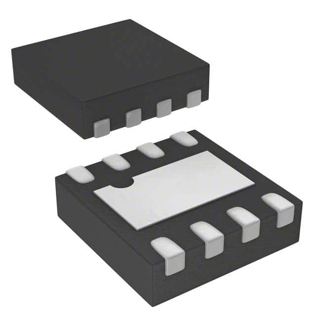
STMicroelectronics TS488IQT
- Part No.:
- TS488IQT
- Manufacturer:
- STMicroelectronics
- Category:
- Audio Amplifiers
- Package:
- 8-UDFN Exposed Pad
- Datasheet:
-
 TS488IQT.pdf
- Description:
- IC AMP CLASS AB STER 130MW 8DFN
- Quantity:
- Payment:

- Shipping:

Inventory:4,734
Please send an inquiry. Send us your inquiry, and we will respond immediately.
Product details
Overview
TS488IQT from STMicroelectronics is a dual-channel, single-ended stereo headphone amplifier IC designed for low-voltage portable audio systems. It delivers up to 120 mW per channel into 16 Ω at 5 V with ≤0.1% THD+N at 1 kHz, features pop/click noise suppression, operates from 2.2–5.5 V, and achieves ultra-low 10 nA typical standby current. It targets space-constrained mobile and embedded audio interfaces requiring high SNR (105 dB) and strong crosstalk rejection (−102 dB).
For engineers reviewing the TS488IQT datasheet, TS488IQT pinout, TS488IQT application, or TS488IQT equivalent, this page provides verified functional identity, validated DFN8 2×2 mm package mapping, confirmed dual-channel Class-AB architecture with active-low standby control, real-world output power vs. supply voltage curves, and design-meaningful PSRR (70 dB @ 1 kHz) and wake-up time (100 ms) specifications.
Technical Context
The TS488IQT implements a unity-gain-stable, externally resistor-configurable dual op-amp architecture optimized for capacitive-coupled headphone drive. Its internal pop/click suppression circuitry actively manages bias sequencing during power-up/down, eliminating transient artifacts without requiring external mute logic.
It supports flexible gain setting via external Rin/Rfeed networks (AV = −Rfeed/Rin), maintains stable operation into 16–600 Ω loads, and integrates short-circuit protection with thermal shutdown. The DFN8 package enables compact PCB layout while delivering 40 °C/W junction-to-ambient thermal resistance on a 4-layer board.
Key Specifications
| Parameter | Value and Actual Design Meaning |
|---|---|
| Supply Voltage Range | 2.2 V to 5.5 V - Enables direct integration with Li-ion battery (3.3 V/3.7 V nominal) and USB-powered (5 V) audio subsystems. |
| Output Power (16 Ω) | 120 mW @ 5 V, 0.1% THD+N - Sufficient for loud, distortion-free playback on standard 16 Ω earbuds. |
| Standby Current | 10 nA typical - Allows multi-week battery life in always-on audio monitoring or voice-assistant wake-up circuits. |
| SNR (A-weighted) | 105 dB @ 5 V, 32 Ω - Ensures high-fidelity audio reproduction with negligible background noise floor. |
| Crosstalk Rejection | −102 dB @ 1 kHz - Prevents audible left/right channel leakage in stereo headphone applications. |
| PSRR | 70 dB @ 1 kHz, 5 V - Rejects ripple from noisy DC-DC converters without requiring ultra-low-noise LDOs. |
| Wake-up Time | 100 ms - Defines maximum latency between standby exit and full audio output readiness. |
Pinout & Package
TS488IQT is housed in a thermally enhanced DFN8 (2 mm × 2 mm, 0.5 mm pitch) package with exposed thermal pad (EP) connected to GND for optimal heat dissipation. Pin 1 is marked by a dot or beveled corner.
| Pin/Terminal | Circuit Role | Design Meaning |
|---|---|---|
| 1 (STDBY) | Active-low standby control input | Pulling low disables amplifier outputs and reduces ICC to 10 nA; high enables normal operation. |
| 2 (IN1−) | Inverting input of Channel 1 | Accepts differential or single-ended audio signal; gain set jointly with Rfeed1. |
| 3 (OUT1) | Channel 1 output | Drives left-channel load via AC-coupling capacitor; capable of ±2.25 V swing into 16 Ω @ 5 V. |
| 4 (GND) | Analog ground reference | Common return path for inputs, outputs, and bypass capacitors; must be low-impedance plane. |
| 5 (VCC) | Positive supply rail | Accepts 2.2–5.5 V; requires local 1 µF ceramic bypass capacitor to GND near pin. |
| 6 (IN2−) | Inverting input of Channel 2 | Accepts right-channel audio signal; independent gain configuration from Channel 1. |
| 7 (OUT2) | Channel 2 output | Drives right-channel load; matched performance to OUT1 ensures stereo balance. |
| 8 (EP) | Exposed thermal pad | Internally connected to GND; must be soldered to PCB copper pour for thermal management (RthJA = 40 °C/W). |
Key Features
| Feature | Design Value |
|---|---|
| Pop & click noise suppression | Integrated analog sequencing eliminates turn-on/off transients without external mute switches or firmware delays. |
| Ultra-low standby current | 10 nA typical enables >1-year battery life in always-listening wearable devices using coin-cell batteries. |
| High PSRR (70 dB @ 1 kHz) | Reduces need for dedicated low-noise LDOs; allows direct use of switched-mode power supplies in portable designs. |
| Unity-gain stable architecture | Supports stable operation with external gain-setting resistors (no compensation capacitor required). |
| Short-circuit protection | Withstands continuous output short to VCC or GND without latch-up or permanent damage. |
Applications
| Mobile Headphone Interface | USB-C Audio Dongle |
|---|---|
Use Scenario: Driving stereo earbuds from a smartphone baseband processor's line-out or DAC output. IC Role / Device Role / Timing Role: Dual-channel audio power amplifier with integrated pop suppression and standby control. Use Value: Eliminates external mute circuitry and reduces BOM count by 3–4 passive components per channel. |
Use Scenario: Audio interface in compact USB-C to 3.5 mm adapter with no internal battery. IC Role / Device Role / Timing Role: Low-quiescent-current headphone driver powered directly from USB 5 V bus. Use Value: Delivers 120 mW/channel at 5 V while consuming only 2.7 mA active current, minimizing host port loading. |
| Smart Speaker Voice Prompt | Industrial Handheld Terminal |
Use Scenario: Playing short voice prompts (e.g., "Ready", "Error") through integrated mono speaker or headset jack. IC Role / Device Role / Timing Role: Standby-enabled audio amplifier triggered by MCU GPIO for burst-mode audio playback. Use Value: 10 nA standby current extends device runtime between voice events; 100 ms wake-up ensures prompt response. |
Use Scenario: Audio feedback in rugged handheld scanners or data collectors operating from 3.3 V main rail. IC Role / Device Role / Timing Role: Robust headphone driver tolerant of industrial temperature range (−40 to +85 °C). Use Value: Maintains 55 mW/channel into 16 Ω at 3.3 V with <0.1% THD+N, ensuring clear audio in noisy environments. |
Equivalent & Alternatives
The following parts are listed as comparable options for similar dual-channel headphone amplifier applications.
| Alternative Part | Technical Difference | Application Difference | Selection Advice |
|---|---|---|---|
| MAX98357AETE+T | I²S-input Class D amplifier; no analog inputs; fixed 12 dB gain; requires external MCLK. | Better efficiency (>90%) but higher EMI risk; unsuitable for analog line-in sources. | Select when system uses digital audio interface and prioritizes battery life over analog flexibility. |
| TAS5707PAG | 4-channel, I²S-input Class D amplifier with integrated DSP; larger HTQFP-64 package; 3.3 V only. | Supports multi-zone audio and parametric EQ but over-specified for simple stereo headphone drive. | Select only if future expansion to 4-channel or audio processing is planned; adds cost and complexity. |
Compared with TS488IQT, MAX98357A offers superior efficiency but lacks analog input support and pop suppression; TAS5707PAG provides advanced features at the cost of size, voltage inflexibility, and unnecessary channel count-making TS488IQT optimal for compact, analog-input, low-quiescent-current stereo headphone applications.
Availability
TS488IQT is available at Aetrix Electronics and suitable for mobile phone audio subsystems, USB-C audio adapters, smart speaker voice prompt modules, and industrial handheld terminals requiring stable component supply across extended temperature ranges (−40 to +85 °C).
Supply support for TS488IQT includes scheduled delivery planning, volume procurement assistance, BOM continuity management, traceable sourcing, and lifecycle availability coordination for OEM customers, industrial embedded developers, connected-device designers, and electronics production programs.
Manufacturer
STMicroelectronics is a global semiconductor leader headquartered in Geneva, Switzerland, designing and manufacturing analog, microcontroller, power, and sensor solutions for automotive, industrial, and consumer markets.
The TS488 belongs to ST's low-power audio amplifier product line, engineered specifically for battery-operated portable devices demanding high audio fidelity, minimal quiescent current, and robust pop/click immunity in miniature packages.
FAQ
What is the minimum recommended output coupling capacitor value for TS488IQT driving 16 Ω headphones?
The datasheet specifies Cout forms a high-pass filter with RL: Fc = 1/(2π × RL × Cout). For 20 Hz cutoff into 16 Ω, Cout ≥ 498 µF. ST recommends ≥100 µF ceramic or polymer capacitor to ensure stability and low distortion across temperature and voltage.
Can TS488IQT drive 32 Ω headphones at 3.3 V with acceptable THD+N?
Yes. At 3.3 V and 32 Ω, TS488IQT delivers 34 mW per channel at 0.1% THD+N (1 kHz). This meets typical headphone sensitivity requirements (≥105 dB SPL/mW), providing adequate loudness with low distortion for most consumer-grade 32 Ω earbuds.
Is the exposed thermal pad (Pin 8) electrically connected internally?
Yes. The exposed pad (EP) is internally tied to GND. It must be soldered to a PCB GND copper pour with ≥4 thermal vias (0.3 mm diameter) to achieve the specified RthJA = 40 °C/W on a 4-layer board. Leaving it unconnected degrades thermal performance and risks thermal shutdown.
Does TS488IQT require external compensation components for stability?
No. TS488IQT is unity-gain stable and does not require external compensation capacitors. Stability is ensured across all gains set by external Rin/Rfeed networks (AV = −Rfeed/Rin) and load conditions from 16 Ω to 600 Ω, per Figure 2–11 in DS4579 Rev 8.
TS488IQT Specifications
- Product attributes
- Attribute value
- Manufacturer:
- STMicroelectronics
- Series:
- -
- Package/Case:
- 8-UDFN Exposed Pad
- Packaging:
- Tape & Reel (TR)
- Product Status:
- Last Time Buy
- Type:
- Class AB
- Output Type:
- Headphones, 2-Channel (Stereo)
- Max Output Power x Channels @ Load:
- 130mW x 2 @ 16Ohm
- Voltage - Supply:
- 2.2V ~ 5.5V
- Features:
- Depop, Short-Circuit Protection, Standby
- Mounting Type:
- Surface Mount
- Operating Temperature:
- -40°C ~ 85°C (TA)
- Grade:
- -
- Qualification:
- -
- Supplier Device Package:
- 8-DFN (2x2)
TS488IQT FAQ
1.How can I place an order for TS488IQT through Aetrix?
Please submit a Request for Quotation (RFQ) for TS488IQT on Aetrix. Our sales agent will provide a competitive quotation and guide you through the order confirmation once you accept the terms.
2.Are the price and stock information for TS488IQT reliable?
The price and inventory of TS488IQT are updated periodically and may fluctuate due to market conditions. Stock and pricing data are typically refreshed every 24 hours. Quotation validity for TS488IQT is usually 5 days.
3.What payment methods are accepted for TS488IQT?
We accept Wire Transfer, PayPal, Credit Card, Western Union, MoneyGram, and Escrow for TS488IQT transactions.
Note: Certain payment methods may incur a processing fee.
4.How is shipping managed for TS488IQT?
TS488IQT orders can be shipped via leading logistics carriers, including DHL, UPS, FedEx, TNT, or Registered Mail.
Once your TS488IQT order is processed, you will receive an email with the shipment details and tracking number.
Note: Tracking information may take up to 24 hours to appear. Express delivery typically takes 3–5 business days.
5.How can I obtain technical support or documentation for TS488IQT?
For technical support, including TS488IQT datasheets, pinout diagrams, or application guidance, please contact our engineering support team. They can provide detailed documentation and assistance for your TS488IQT requirements.
6.How does Aetrix verify that TS488IQT is sourced from the original manufacturer or authorized distributors?
All TS488IQT products on Aetrix are procured from qualified distributors and authorized channels. Our dedicated quality assurance team conducts strict verification, including traceability checks and, if necessary, third-party testing. This ensures that TS488IQT meets industry standards.
7.What is the process for return or replacement of TS488IQT?
All TS488IQT units undergo pre-shipment inspection (PSI). If there is an issue with TS488IQT, returns or replacements are accepted under the following conditions:
1.Quantity discrepancies, incorrect items, or visible external defects (such as breakage or corrosion), acknowledged by Aetrix.
2.The issue is reported within 90 days of delivery.
3.The TS488IQT part is unused and in its original packaging.
Return procedure for TS488IQT:
1.Submit a request within 90 days.
2.Obtain a Return Material Authorization (RMA) from Aetrix.
TS488IQT Tags
-Exposed-Pad.jpg)
-
TS34119CS RLG
Taiwan Semiconductor Corporation

-
LM386MX-1/NOPB
Texas Instruments

-
TPA711DGNR
Texas Instruments

-
LM386N-4/NOPB
Texas Instruments

-
TS4990IST
STMicroelectronics
-
PAM8302AASCR
Diodes Incorporated
-
TPA6130A2RTJR
Texas Instruments
-
TPA6111A2DGNR
Texas Instruments
-
LM4861MX/NOPB
Texas Instruments
-
LM386M-1/NOPB
Texas Instruments

-
NCS2211DR2G
onsemi
-
IS31AP2005-DLS2-TR
Lumissil Microsystems
Tech Hub

A practical engineering and sourcing framework covering lifecycle verification, lifetime-buy calculations, replacement qualification, supplier checks and counterfeit-risk controls.

TTL and CMOS logic families differ in thresholds, loading, output drive, power and timing. This engineering guide compares 74HC and 74HCT, calculates noise margins and checks 3.3 V/5 V compatibility.

A practical engineering guide to 3.3V and 5V logic compatibility, input thresholds, resistor dividers, translator ICs, MOSFET level shifting, I2C pull-ups, timing limits and power-sequencing risks.

The 74HC595 uses push-pull logic outputs, while the TPIC6B595 uses 50 V open-drain DMOS sinks for higher-power loads. This guide compares timing, current limits, 3.3 V interfacing, load wiring, thermal…

The 74HC595 converts serial data into eight stable parallel outputs. This guide covers pin functions, shift and storage timing, OE and MR behavior, drive-current limits, cascading, voltage compatibilit…

A technical comparison of level-sensitive latches and edge-triggered flip-flops, covering timing windows, setup and hold limits, master–slave operation, time borrowing, race-through, HDL inference and…

A D latch stores one bit while Enable controls when data can pass. This reference covers gate-level operation, truth tables, transparency, setup and hold timing, LE versus OE, common ICs and practical …

An SR latch stores one bit through cross-coupled feedback. This engineering reference covers NOR and NAND implementations, truth tables, forbidden-state recovery, gated operation, switch debouncing, fa…

Latch circuits retain one bit through feedback. This technical reference covers SR and D latches, truth tables, transparency, timing limits, latch-versus-flip-flop behavior, applications and common log…

An engineering guide to LED driver operation, constant-current and constant-voltage outputs, linear and switching topologies, dimming, IC selection, calculations, replacement compatibility, and fault c…


