
 My Inquiry
 My Account


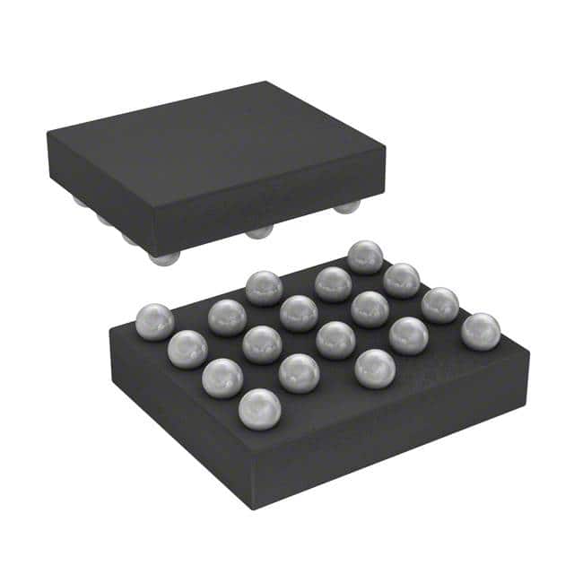
STMicroelectronics TS4956EIJT
- Part No.:
- TS4956EIJT
- Manufacturer:
- STMicroelectronics
- Category:
- Audio Amplifiers
- Package:
- 18-UFBGA, FCBGA
- Datasheet:
-
 TS4956EIJT.pdf
- Description:
- IC AMP AB MONO 1W 18FLIPCHIP
- Quantity:
- Payment:

- Shipping:

Inventory:2,600
Please send an inquiry. Send us your inquiry, and we will respond immediately.
Product details
Overview
TS4956EIJT from STMicroelectronics is a stereo audio amplifier system with integrated I²C bus interface, delivering 38 mW per channel into 16 Ω at 3.3 V (1% THD+N), supporting eight configurable output modes including BTL speaker drive, phantom-ground headphone, and mono line-out, and featuring ultra-low 0.5 µA standby current for mobile handset power management.
For engineers reviewing the TS4956EIJT datasheet, TS4956EIJT pinout, TS4956EIJT application, or TS4956EIJT equivalent, this device is selected for compact portable audio systems requiring digital gain control, pop/click suppression, thermal shutdown protection, and multi-output flexibility without external analog switches or discrete amplifiers.
Technical Context
The TS4956EIJT integrates three independent amplifier paths-stereo headphone (LHP/RHP), mono loudspeaker (MLO), and mono line-out (PHG)-each selectable via I²C register writes. Its 8-mode configuration includes BTL (modes 1/2/7), phantom-ground (modes 3/4), and single-ended (modes 5/6), with gain programmable from –34.5 dB to +12 dB in 1.5 dB steps.
It implements flip-chip packaging with 18 bumps, uses internal half-supply biasing (via BYPASS capacitor), and features dedicated I²C supply (I2CVCC) enabling true zero-power standby when grounded. Thermal shutdown activates at 150 °C, and PSRR exceeds 73 dB in BTL mode at 217 Hz.
Key Specifications
| Parameter | Value and Actual Design Meaning |
|---|---|
| Supply voltage | 2.7 V to 5.5 V - supports Li-ion battery operation and USB-powered designs without LDO pre-regulation. |
| Headphone output power | 38 mW @ 16 Ω, 1 kHz, 1% THD+N at 3.3 V - sufficient for loud listening on standard earbuds without clipping. |
| BTL speaker output power | 450 mW @ 8 Ω, 1 kHz, 1% THD+N at 3.3 V - drives small speakers directly with minimal external components. |
| Digital volume control | 32-step range from +12 dB to –34.5 dB - enables precise loudness matching across diverse audio sources and transducers. |
| I²C interface | 400 kHz fast-mode, slave-only, separate I2CVCC pin - isolates logic-level compatibility from main VCC rail and enables deep-sleep control. |
| Standby current | 0.5 µA typical - reduces battery drain during call idle or media pause states in handheld devices. |
| THD+N | 0.5% max (20 Hz–20 kHz) - meets consumer audio fidelity requirements for voice and music playback. |
| PSRR | 77 dB (mode 4, 217 Hz) - rejects switching noise from PMICs and DC-DC converters in noisy portable power domains. |
Pinout & Package
TS4956EIJT uses a lead-free flip-chip package with 18 bumps (300 µm diameter), mounted face-down with solder bumps forming electrical connections; thermal resistance junction-to-ambient is 90 °C/W with 120 mm² heat sink surface.
| Pin/Terminal | Circuit Role | Design Meaning |
|---|---|---|
| RIN | Stereo right input | Differential-capable input node; referenced to ground with 30 kΩ impedance in stereo mode. |
| LHP- | Left headphone negative output | Phantom-ground output terminal; forms differential pair with LHP+ for low-THD headphone drive. |
| MLO | Mono loudspeaker output | Single-ended output capable of 65 mW into 16 Ω; used in hands-free or auxiliary speaker applications. |
| RHP+ | Right headphone positive output | Phantom-ground output terminal; paired with RHP− to deliver balanced drive to stereo headphones. |
| MIN | Mono input negative | Inverting input for mono differential source; 24 kΩ impedance referenced to ground. |
| VCC | Main power supply | Supplies all amplifier stages and internal logic; must be ≥2.7 V and not grounded for I²C functionality. |
| SDA | I²C serial data | Open-drain bidirectional line; requires external pull-up; carries register read/write commands and status data. |
| LIN | Stereo left input | Differential-capable input node; 30 kΩ impedance referenced to ground in stereo mode. |
| GND | Ground reference | Common return path for analog and digital sections; critical for PSRR and crosstalk performance. |
| I2CVCC | I²C interface supply | Independent power rail for I²C logic; grounding disables I²C and forces 0.5 µA standby state. |
| MIP | Mono input positive | Non-inverting mono input; 24 kΩ impedance; used with MIN for differential microphone or line-level signals. |
| SRP+ | Speaker right positive (BTL) | BTL output phase for right channel; driven 180° out-of-phase with SRN− to double effective voltage swing. |
| SRN- | Speaker right negative (BTL) | BTL output phase for right channel; complements SRP+ to deliver 4× power vs. single-ended into same load. |
| SCL | I²C clock input | Open-drain clock line; synchronized with SDA; defines timing for register access and mode updates. |
| BYPASS | Half-supply decoupling | Connects to 1 µF capacitor to generate stable internal VCC/2 bias for AC-coupled outputs. |
| PGH | Phantom ground output | Internal bias node for headphone outputs; eliminates need for external DC-blocking capacitors in PHG mode. |
Key Features
| Feature | Design Value |
|---|---|
| 8 programmable output configurations | Selects BTL speaker, phantom-ground headphone, or mono line-out via I²C register bits D2–D0 - eliminates external mode-switching hardware. |
| Pop-and-click reduction circuitry | Hardware-based soft-start and mute sequencing - prevents audible transients during power-up, mode change, or volume adjustment. |
| Output power limitation (headphone) | Internal limiter caps headphone output to safe eardrum levels - avoids need for external compression or monitoring circuits. |
| Thermal shutdown protection | Activates at 150 °C junction temperature and auto-recovers - protects device and PCB during sustained high-power operation. |
| 32-step digital volume control | 1.5 dB resolution with ±0.6 dB step accuracy - enables consistent loudness scaling across multiple audio sources and codecs. |
| Ultra-low standby current | 0.5 µA with I2CVCC = GND - extends battery life in always-on voice assistant or alarm-clock applications. |
Applications
| Mobile Handset Audio | Tablet Media Playback |
|---|---|
|
Use Scenario: Dual-path audio routing in GSM/UMTS smartphones supporting simultaneous headset playback and loudspeaker notification. IC Role / Device Role / Timing Role: Audio system hub managing stereo headphone, mono speaker, and hands-free line-out under real-time I²C command from baseband processor. Use Value: Eliminates three discrete amplifiers and analog switches; reduces BOM count by 7 components and PCB area by >25 mm². |
Use Scenario: High-fidelity stereo playback from Android/iOS tablets with dynamic output reconfiguration (e.g., switch from headphones to docked speaker). IC Role / Device Role / Timing Role: Single-chip audio driver providing BTL speaker output (mode 7) and phantom-ground headphone output (mode 4) with <90 ms wake-up latency. Use Value: Enables seamless audio path switching without audible artifacts or MCU firmware intervention - improves UX responsiveness. |
| Portable VoIP Terminal | Wearable Voice Assistant |
|
Use Scenario: SIP-based cordless phone with hands-free speakerphone, headset jack, and ringtone loudspeaker in one enclosure. IC Role / Device Role / Timing Role: Multi-output audio subsystem handling full-duplex voice (MIP/MIN inputs), local playback (RIN/LIN), and alert tones (MLO). Use Value: Integrates 3 independent amplifiers with shared I²C control - simplifies layout and eliminates inter-channel crosstalk from discrete solutions. |
Use Scenario: Compact smart speaker with embedded voice assistant requiring low-power headphone output and occasional speaker boost. IC Role / Device Role / Timing Role: Low-quiescent audio driver operating in mode 4 (headphone) during user interaction and mode 1 (BTL speaker) for alarms or notifications. Use Value: Achieves 0.5 µA standby and <1 µs shutdown exit - extends battery runtime beyond 72 hours in listen-for-wake-word mode. |
Equivalent & Alternatives
The following parts are listed as comparable options for similar stereo audio amplifier applications.
| Alternative Part | Technical Difference | Application Difference | Selection Advice |
|---|---|---|---|
| MAX9850ETJ+T | Fixed 2.5 W BTL output, no headphone path, I²C-controlled but lacks phantom-ground mode and MLO output. | Targeted at speaker-only portable systems; cannot replace TS4956EIJT in dual-path (headphone + speaker) designs. | Select only if application requires higher speaker power (>450 mW) and omits headphone or line-out functionality. |
| TAS5706PAPR | Class-D, 3 W/channel, I²S input, no integrated headphone amplifier or I²C volume control; requires external DAC and level-shifting. | Suitable for AC-powered docking stations; incompatible with battery-powered, space-constrained handhelds needing integrated analog inputs/outputs. | Choose when system already uses I²S audio interface and prioritizes efficiency over integration density and analog flexibility. |
Compared with MAX9850ETJ+T and TAS5706PAPR, the TS4956EIJT uniquely combines stereo headphone drive, BTL speaker output, mono line-out, and I²C-configurable gain/mode in a single flip-chip IC - making it irreplaceable in compact, multi-interface mobile audio subsystems.
Availability
TS4956EIJT is available at Aetrix Electronics and suitable for mobile handsets, tablet media subsystems, portable VoIP terminals, and wearable voice assistants requiring stable component supply and long-lifecycle support.
Supply support for TS4956EIJT includes scheduled delivery planning, volume procurement assistance, BOM continuity management, traceable sourcing, and lifecycle availability coordination for OEM customers, industrial embedded developers, connected-device designers, and electronics production programs.
Manufacturer
STMicroelectronics is a global semiconductor leader headquartered in Geneva, Switzerland, designing and manufacturing analog, mixed-signal, power, and microcontroller products for industrial, automotive, and consumer markets.
The TS4956EIJT belongs to ST's low-voltage audio amplifier product line, engineered specifically for space-constrained portable electronics requiring multi-output flexibility, ultra-low power management, and robust I²C configurability.
FAQ
What is the minimum recommended bypass capacitor value on the BYPASS pin?
A 1 µF ceramic capacitor is required between BYPASS and GND to stabilize the internal half-supply bias generator. Using less than 1 µF causes increased THD+N and reduced PSRR, especially below 100 Hz. The capacitor must be placed within 2 mm of the BYPASS pin with low-inductance layout to prevent oscillation in phantom-ground output modes.
Can TS4956EIJT operate with VCC = 2.5 V?
No. Absolute maximum ratings specify VCC must not fall below 2.7 V. At 2.5 V, the internal bias circuit fails to establish proper phantom-ground voltage, causing severe distortion (>5% THD+N) and potential latch-up. Operation below 2.7 V voids specification compliance and may damage the device under transient load conditions.
How does the I2CVCC pin affect I²C communication reliability?
I2CVCC must be tied to a stable 2.7–5.5 V supply independent of VCC. If I2CVCC is unconnected or floating, SDA/SCL pins enter undefined logic states, causing I²C bus lockup. Grounding I2CVCC forces 0.5 µA standby and disables all I²C response - this is intentional for zero-power sleep, not a fault condition.
Is thermal derating required when using TS4956EIJT in mode 7 (BTL) at 5 V?
Yes. At VCC = 5 V and 8 Ω load, mode 7 draws up to 8.7 mA quiescent current and delivers ~1.2 W dissipation under full output. With Rthja = 90 °C/W, junction temperature rises ~108 °C above ambient - exceeding 150 °C limit at Tamb > 42 °C. A 120 mm² copper pour is mandatory; forced air or thermal vias are recommended for continuous operation above 35 °C ambient.
TS4956EIJT Specifications
- Product attributes
- Attribute value
- Manufacturer:
- STMicroelectronics
- Series:
- -
- Package/Case:
- 18-UFBGA, FCBGA
- Packaging:
- Tape & Reel (TR)
- Product Status:
- Obsolete
- Type:
- Class AB
- Output Type:
- 1-Channel (Mono) with Mono and Stereo Headphones
- Max Output Power x Channels @ Load:
- 1W x 1 @ 8Ohm; 43mW x 2 @ 32Ohm
- Voltage - Supply:
- 2.7V ~ 5.5V
- Features:
- Depop, Differential Inputs, I2C, Shutdown, Standby, Thermal Protection, Volume Control
- Mounting Type:
- Surface Mount
- Operating Temperature:
- -40°C ~ 85°C (TA)
- Grade:
- -
- Qualification:
- -
- Supplier Device Package:
- 18-FlipChip
TS4956EIJT FAQ
1.How can I place an order for TS4956EIJT through Aetrix?
Please submit a Request for Quotation (RFQ) for TS4956EIJT on Aetrix. Our sales agent will provide a competitive quotation and guide you through the order confirmation once you accept the terms.
2.Are the price and stock information for TS4956EIJT reliable?
The price and inventory of TS4956EIJT are updated periodically and may fluctuate due to market conditions. Stock and pricing data are typically refreshed every 24 hours. Quotation validity for TS4956EIJT is usually 5 days.
3.What payment methods are accepted for TS4956EIJT?
We accept Wire Transfer, PayPal, Credit Card, Western Union, MoneyGram, and Escrow for TS4956EIJT transactions.
Note: Certain payment methods may incur a processing fee.
4.How is shipping managed for TS4956EIJT?
TS4956EIJT orders can be shipped via leading logistics carriers, including DHL, UPS, FedEx, TNT, or Registered Mail.
Once your TS4956EIJT order is processed, you will receive an email with the shipment details and tracking number.
Note: Tracking information may take up to 24 hours to appear. Express delivery typically takes 3–5 business days.
5.How can I obtain technical support or documentation for TS4956EIJT?
For technical support, including TS4956EIJT datasheets, pinout diagrams, or application guidance, please contact our engineering support team. They can provide detailed documentation and assistance for your TS4956EIJT requirements.
6.How does Aetrix verify that TS4956EIJT is sourced from the original manufacturer or authorized distributors?
All TS4956EIJT products on Aetrix are procured from qualified distributors and authorized channels. Our dedicated quality assurance team conducts strict verification, including traceability checks and, if necessary, third-party testing. This ensures that TS4956EIJT meets industry standards.
7.What is the process for return or replacement of TS4956EIJT?
All TS4956EIJT units undergo pre-shipment inspection (PSI). If there is an issue with TS4956EIJT, returns or replacements are accepted under the following conditions:
1.Quantity discrepancies, incorrect items, or visible external defects (such as breakage or corrosion), acknowledged by Aetrix.
2.The issue is reported within 90 days of delivery.
3.The TS4956EIJT part is unused and in its original packaging.
Return procedure for TS4956EIJT:
1.Submit a request within 90 days.
2.Obtain a Return Material Authorization (RMA) from Aetrix.
TS4956EIJT Tags
-Exposed-Pad.jpg)
-
TS34119CS RLG
Taiwan Semiconductor Corporation

-
LM386MX-1/NOPB
Texas Instruments

-
TPA711DGNR
Texas Instruments

-
LM386N-4/NOPB
Texas Instruments

-
TS4990IST
STMicroelectronics
-
PAM8302AASCR
Diodes Incorporated
-
TPA6130A2RTJR
Texas Instruments
-
TPA6111A2DGNR
Texas Instruments
-
LM4861MX/NOPB
Texas Instruments
-
LM386M-1/NOPB
Texas Instruments

-
NCS2211DR2G
onsemi
-
IS31AP2005-DLS2-TR
Lumissil Microsystems
Tech Hub

An engineering guide to LED driver operation, constant-current and constant-voltage outputs, linear and switching topologies, dimming, IC selection, calculations, replacement compatibility, and fault c…

Operational amplifier guide covering op amp basics, feedback, ideal vs real op amps, common configurations, buffer circuits, offset, bias current, gain-bandwidth, slew rate, rail-to-rail limits and sel…

Jumper cables guide covering safe connection order, red and black clamp placement, final ground connection, cable gauge, length, clamp quality, copper vs CCA cables, jump starter comparison and battery…

LDO regulator guide covering low dropout voltage, power dissipation, thermal design, PSRR, output noise, capacitor stability, adjustable LDO circuits, LDO vs buck converter and datasheet selection chec…

Conditional Access Module guide covering CAM meaning, CI/CI+ interface, smart card authorization, DVB security workflow, TV and set-top box compatibility, internal electronics, ESD protection, connecto…

Guide to electronic component obsolescence covering EOL risk, PCN/PDN notices, last-time buy planning, replacement options, form-fit-function validation, counterfeit risk and BOM lifecycle management.

18650 battery guide covering lithium-ion cell basics, 3.6V/3.7V voltage, 4.2V charging, mAh and Wh capacity, protected cells, chargers, BMS, series-parallel packs, holders, welding and sourcing checks.…

Hall effect sensor guide covering working principle, linear and digital sensors, Arduino circuits, current sensing, speed detection, automotive applications, A3144 examples, signal filtering and datash…

Product Change Notification guide for electronic components, covering PCN meaning, PCN vs PDN/EOL, common change types, risk levels, form-fit-function review, engineering validation, BOM control, LTB/L…

A practical guide to blend door actuators, covering HVAC function, symptoms, location, AC and heater issues, reset and calibration, replacement cost, electrical diagnosis, compatibility checks, and rep…


