
 My Inquiry
 My Account


Texas Instruments TWL6030B1AACMR
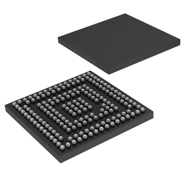
- Part No.:
- TWL6030B1AACMR
- Manufacturer:
- Texas Instruments
- Category:
- Power Management - Specialized
- Package:
- -
- Datasheet:
-
 TWL6030B1AACMR.pdf
- Description:
- IC POWER MGMT SW MODE CHRGR
- Quantity:
- Payment:

- Shipping:

Inventory:2,248
Please send an inquiry. Send us your inquiry, and we will respond immediately.
Product details
Overview
TWL6030B1AACMR from Texas Instruments is a fully integrated power management IC (PMIC) designed for OMAP4460/4470-based mobile systems. It delivers seven 6-MHz buck converters (two at 1.6 A, five at 1.0 A), 11 LDOs, a 1.5-A switched-mode battery charger, USB OTG support, RTC with alarm wake-up, and 10-bit/13-bit ADCs - enabling complete power sequencing and system-level power control in smartphones and tablets.
For engineers reviewing the TWL6030B1AACMR datasheet, TWL6030B1AACMR pinout, TWL6030B1AACMR application, or TWL6030B1AACMR equivalent, key selection criteria include its OMAP4460/4470 compatibility, watchdog-enabled power-up sequence, tape-and-reel packaging (2500-unit reels), and nFBGA-187 package with 0.4-mm ball pitch for high-density portable designs.
Technical Context
The TWL6030B1AACMR implements a programmable EPROM-based power-up/power-down controller supporting custom sequencing across all seven SMPS and 11 LDOs. Its dual I²C interfaces (CTL and SmartReflex) enable independent configuration of power rails and dynamic voltage scaling for processor cores (VCORE1–VCORE3), memory (VMEM), and I/O (V1V8, V2V1).
It integrates a 32-kHz crystal oscillator with three gated clock outputs (CLK32KAO, CLK32KAUDIO, CLK32KG), thermal monitoring with high-temperature warning and shutdown, and a Coulomb counter with four programmable integration periods for precise battery fuel gauging - all operating from a single-cell Li-Ion/Li-Polymer supply (2.5–4.8 V).
Key Specifications
| Parameter | Value and Actual Design Meaning |
|---|---|
| Package | 187-ball nFBGA, 7.0 mm × 7.0 mm, 0.4-mm ball pitch - optimized for compact smartphone PCB layouts |
| Buck Converters | Seven 6-MHz SMPS: two rated at 1.6 A (VCORE1, VCORE2), five at 1.0 A (VCORE3, VMEM, V1V8, V2V1, V1V29) - supports high-efficiency core/memory rail regulation |
| LDO Count | 11 LDOs including VANA (0.2 A), VUSB (35 mA), VAUXx (vibrator driver), and internal-use regulators - provides low-noise bias for analog/audio subsystems |
| Battery Charger | 1.5-A switched-mode charger with integrated FET, thermal regulation, safety timer, and LED driver - enables fast, safe charging without external components |
| ADC & Gauging | 10-bit GPADC (17 channels), 13-bit Coulomb counter with four integration periods - enables real-time battery state-of-charge and system monitoring |
| Power Sequencing | EPROM-programmable startup/shutdown sequences with three configurable event signals - ensures reliable boot and controlled power-down for OMAP4 platforms |
| Watchdog | Enabled watchdog timer per Table 1 - provides hardware-level system reset supervision for OMAP4460/4470 applications |
Pinout & Package
Package: 187-pin nFBGA (7.0 mm × 7.0 mm, 0.4-mm ball pitch), RoHS-compliant, moisture sensitivity level 3.
| Pin/Terminal | Circuit Role | Design Meaning |
|---|---|---|
| VIO | Digital I/O supply | 1.8-V input for all digital logic; defines voltage level for CTLI2C and SRI2C interfaces |
| CTLI2C_SDA / CTLI2C_SCL | Main configuration interface | Two-wire I²C bus for PMIC register programming, power rail setup, and sequencing control |
| VCORE1_SW / VCORE1_FDBK | Core power switch node & feedback | High-side switch output and precision feedback path for VCORE1 SMPS (1.6 A, 0.6–2.1 V) |
| CHRG_PMID / CHRG_SW | Charger power path | Midpoint connection and switching node for integrated 1.5-A battery charger FETs |
| CLK32KAO / CLK32KG | 32-kHz clock outputs | Always-on and software-gated 32-kHz clocks for RTC, audio, and system timing domains |
| GPADC_IN0–GPADC_IN6 | Analog sensor inputs | Seven dedicated ADC channels for battery voltage, temperature, headset detection, and system monitoring |
Key Features
| Feature | Design Value |
|---|---|
| Configurable Power Sequencing | EPROM-programmable startup/shutdown order across all SMPS and LDOs - eliminates need for external sequencer in OMAP4 designs |
| Integrated USB OTG Module | Complies with USB 2.0, OTG/EH 2.0, and USB Battery Charging 1.1/1.2 - enables host/peripheral mode without external transceivers |
| Backup Battery Charger | Dedicated circuit for VBACKUP (1.9–4.8 V) - maintains RTC and alarm functionality during main battery removal |
| Thermal Monitoring | On-die temperature sensor with high-temp warning and automatic thermal shutdown - protects against sustained overloads in sealed handheld enclosures |
| SmartReflex Interface | Dedicated SRI2C bus for dynamic voltage/frequency scaling coordination with OMAP4 processors - reduces active power by up to 30% in DVFS-aware systems |
Applications
| Smartphone Power Management | Tablet System Power |
|---|---|
Use Scenario: Primary PMIC in OMAP4460/4470-based smartphones requiring multi-rail sequencing, fast charging, and low-power standby. IC Role / Device Role / Timing Role: Central power controller managing VCOREx, VMEM, VIO, and peripheral LDOs; provides 32-kHz RTC clock and wake-up alarms. Use Value: Reduces BOM count by integrating 7 SMPS + 11 LDOs + charger + ADC + RTC - eliminates discrete power solutions and saves >15 mm² PCB area. | Use Scenario: Power subsystem for 7–10 inch Android tablets with dual-core Cortex-A9 processors and high-resolution displays. IC Role / Device Role / Timing Role: Supplies core, memory, display I/O, and USB OTG rails; manages thermal throttling and battery gauging via integrated Coulomb counter. Use Value: Enables deep-sleep current as low as 110 µA (with two DCDCs active) - extends standby time beyond 14 days on typical tablet batteries. |
| Gaming Handset Platform | Portable Navigation System |
Use Scenario: High-performance gaming handset with GPU-intensive workloads and aggressive thermal constraints. IC Role / Device Role / Timing Role: Delivers dynamically scaled VCORE1/VCORE2 rails under SmartReflex control; monitors die temperature and triggers throttling before 125°C junction limit. Use Value: Maintains sustained GPU performance while limiting peak power draw through coordinated voltage/frequency scaling - prevents thermal throttling-induced frame drops. | Use Scenario: Automotive-grade portable navigation device requiring GPS lock retention, backup power, and cold-temperature operation. IC Role / Device Role / Timing Role: Powers GPS baseband, RF front-end, and display; uses VBACKUP input and RTC alarm to maintain time and location context during engine-off periods. Use Value: Supports VBACKUP operation down to –40°C with <5 µA backup mode current - preserves GPS almanac and last-known position for instant cold-start acquisition. |
Equivalent & Alternatives
The following parts are listed as comparable options for similar PMIC applications.
| Alternative Part | Technical Difference | Application Difference | Selection Advice |
|---|---|---|---|
| TWL6032B1AECMRR | Same OMAP4460/4470 support but watchdog disabled; no EPROM-based power-up sequence customization | Suitable for cost-sensitive designs where fixed sequencing suffices and watchdog supervision is omitted | Select when simplified firmware integration and lower qualification overhead are prioritized over field-upgradable sequencing |
| TPS65950ZCH | Pin-compatible nFBGA-187 package; supports OMAP4 but lacks integrated Coulomb counter and SmartReflex I²C bus | Used in legacy OMAP4 designs requiring identical footprint but with external fuel gauging and manual DVFS coordination | Choose only if existing board layout must be reused and Coulomb counting is handled externally |
Compared with TWL6030B1AACMR, TWL6032B1AECMRR offers identical power architecture but removes watchdog and EPROM configurability - reducing firmware complexity at the cost of field-upgradable sequencing. TPS65950ZCH matches the physical interface but requires external battery gauging and lacks SmartReflex coordination, increasing system-level design effort.
Availability
TWL6030B1AACMR is available at Aetrix Electronics and suitable for smartphone, tablet, and portable navigation systems requiring stable component supply, long-term lifecycle support, and OMAP4460/4470 platform compatibility.
Supply support for TWL6030B1AACMR includes scheduled delivery planning, volume procurement assistance, BOM continuity management, traceable sourcing, and lifecycle availability coordination for OEM customers, industrial embedded developers, connected-device designers, and electronics production programs.
Manufacturer
Texas Instruments is a global semiconductor leader specializing in analog, embedded processing, and power management technologies.
The TWL6030 product line was engineered as a highly integrated PMIC family for OMAP4 application processors - delivering consolidated power, battery management, real-time clock, and system monitoring in a single chip to reduce mobile platform BOM and board space.
FAQ
What is the primary application target for the TWL6030B1AACMR?
The TWL6030B1AACMR is specifically designed for OMAP4460 and OMAP4470 application processors in smartphones, tablets, and gaming handsets. Its EPROM-programmable power sequencing, watchdog timer, and dual I²C interfaces align precisely with OMAP4 platform requirements - making it unsuitable for non-OMAP4 systems without significant firmware adaptation. TWL6030B1AACMR integrates all essential power functions required for these processors, including core/memory rail generation and USB OTG compliance.
Does the TWL6030B1AACMR support USB On-The-Go functionality?
Yes, the TWL6030B1AACMR includes a fully integrated USB OTG module compliant with USB 2.0, OTG/EH 2.0, and USB Battery Charging 1.1/1.2 specifications. It provides VBUS sensing, ID pin detection, SRP support, and boost-mode operation - enabling host/peripheral role switching without external transceivers. This capability is confirmed in the SWCS045C datasheet Section 1 and is implemented via dedicated CHRG_DET_N, ID, and VBUS pins on the nFBGA-187 package used by TWL6030B1AACMR.
What is the significance of the 'B1AAC' suffix in TWL6030B1AACMR?
The 'B1AAC' suffix in TWL6030B1AACMR identifies its specific configuration within the TWL6030 family: OMAP4460/4470 processor support, enabled watchdog timer, and enabled power-up sequence control. Per Table 1 in the SWCS045C datasheet, this variant ships in tape-and-reel packaging (2500 units) and is distinct from B1A0 (watchdog enabled but sequence control disabled) and B1AE (watchdog disabled). The suffix directly maps to functional behavior - not just packaging - and determines firmware initialization requirements for TWL6030B1AACMR.
How does the TWL6030B1AACMR handle battery charging and thermal protection?
The TWL6030B1AACMR implements a 1.5-A switched-mode battery charger with integrated power FETs, safety timer, input/output overvoltage protection, and thermal regulation. When die temperature exceeds thresholds, it automatically reduces charge current or halts charging to prevent damage - verified in the Absolute Maximum Ratings and Electrical Characteristics sections of the SWCS045C datasheet. This thermal protection operates independently of host control and applies specifically to the TWL6030B1AACMR's internal charger circuitry, ensuring safe operation across ambient temperatures from –40°C to 85°C.
Can the TWL6030B1AACMR operate without an external 32-kHz crystal?
No, the TWL6030B1AACMR requires an external 32-kHz crystal connected to OSC32KIN/OSC32KOUT pins to generate its RTC clock and 32-kHz system clocks (CLK32KAO, CLK32KAUDIO, CLK32KG). While the datasheet mentions RC oscillator alternatives in general TWL6030 descriptions, the TWL6030B1AACMR variant - like all members of the family - relies on the crystal for RTC accuracy and alarm wake-up functionality. The OSC32KCAP pin is designated for crystal load capacitance tuning, confirming mandatory crystal use for TWL6030B1AACMR.
TWL6030B1AACMR Specifications
- Product attributes
- Attribute value
- Manufacturer:
- Texas Instruments
- Series:
- -
- Package/Case:
- -
- Packaging:
- Bulk
- Product Status:
- Not For New Designs
- Applications:
- Handheld/Mobile Devices, OMAP™
- Current - Supply:
- 20µA
- Voltage - Supply:
- 2.5V ~ 4.8V
- Operating Temperature:
- -40°C ~ 85°C
- Grade:
- -
- Qualification:
- -
- Mounting Type:
- Surface Mount
- Supplier Device Package:
- 187-FCBGA (7x7)
TWL6030B1AACMR FAQ
1.How can I place an order for TWL6030B1AACMR through Aetrix?
Please submit a Request for Quotation (RFQ) for TWL6030B1AACMR on Aetrix. Our sales agent will provide a competitive quotation and guide you through the order confirmation once you accept the terms.
2.Are the price and stock information for TWL6030B1AACMR reliable?
The price and inventory of TWL6030B1AACMR are updated periodically and may fluctuate due to market conditions. Stock and pricing data are typically refreshed every 24 hours. Quotation validity for TWL6030B1AACMR is usually 5 days.
3.What payment methods are accepted for TWL6030B1AACMR?
We accept Wire Transfer, PayPal, Credit Card, Western Union, MoneyGram, and Escrow for TWL6030B1AACMR transactions.
Note: Certain payment methods may incur a processing fee.
4.How is shipping managed for TWL6030B1AACMR?
TWL6030B1AACMR orders can be shipped via leading logistics carriers, including DHL, UPS, FedEx, TNT, or Registered Mail.
Once your TWL6030B1AACMR order is processed, you will receive an email with the shipment details and tracking number.
Note: Tracking information may take up to 24 hours to appear. Express delivery typically takes 3–5 business days.
5.How can I obtain technical support or documentation for TWL6030B1AACMR?
For technical support, including TWL6030B1AACMR datasheets, pinout diagrams, or application guidance, please contact our engineering support team. They can provide detailed documentation and assistance for your TWL6030B1AACMR requirements.
6.How does Aetrix verify that TWL6030B1AACMR is sourced from the original manufacturer or authorized distributors?
All TWL6030B1AACMR products on Aetrix are procured from qualified distributors and authorized channels. Our dedicated quality assurance team conducts strict verification, including traceability checks and, if necessary, third-party testing. This ensures that TWL6030B1AACMR meets industry standards.
7.What is the process for return or replacement of TWL6030B1AACMR?
All TWL6030B1AACMR units undergo pre-shipment inspection (PSI). If there is an issue with TWL6030B1AACMR, returns or replacements are accepted under the following conditions:
1.Quantity discrepancies, incorrect items, or visible external defects (such as breakage or corrosion), acknowledged by Aetrix.
2.The issue is reported within 90 days of delivery.
3.The TWL6030B1AACMR part is unused and in its original packaging.
Return procedure for TWL6030B1AACMR:
1.Submit a request within 90 days.
2.Obtain a Return Material Authorization (RMA) from Aetrix.
TWL6030B1AACMR Tags

-
TPS2511DGNR
Texas Instruments

-
UTC2000/MG
Microchip Technology

-
TUSB320HAIRWBR
Texas Instruments

-
TPS61252DSGR
Texas Instruments

-
PI5USB30216CXUAEX
Diodes Incorporated

-
SN6501DBVR
Texas Instruments

-
CYPD3177-24LQXQT
Infineon Technologies
-
SN6501QDBVRQ1
Texas Instruments

-
STUSB1600AQTR
STMicroelectronics

-
SN6505BDBVR
Texas Instruments
-
SN6501DBVT
Texas Instruments

-
TPS65150PWPR
Texas Instruments
Tech Hub

A practical engineering guide to 3.3V and 5V logic compatibility, input thresholds, resistor dividers, translator ICs, MOSFET level shifting, I2C pull-ups, timing limits and power-sequencing risks.

The 74HC595 uses push-pull logic outputs, while the TPIC6B595 uses 50 V open-drain DMOS sinks for higher-power loads. This guide compares timing, current limits, 3.3 V interfacing, load wiring, thermal…

The 74HC595 converts serial data into eight stable parallel outputs. This guide covers pin functions, shift and storage timing, OE and MR behavior, drive-current limits, cascading, voltage compatibilit…

A technical comparison of level-sensitive latches and edge-triggered flip-flops, covering timing windows, setup and hold limits, master–slave operation, time borrowing, race-through, HDL inference and…

A D latch stores one bit while Enable controls when data can pass. This reference covers gate-level operation, truth tables, transparency, setup and hold timing, LE versus OE, common ICs and practical …

An SR latch stores one bit through cross-coupled feedback. This engineering reference covers NOR and NAND implementations, truth tables, forbidden-state recovery, gated operation, switch debouncing, fa…

Latch circuits retain one bit through feedback. This technical reference covers SR and D latches, truth tables, transparency, timing limits, latch-versus-flip-flop behavior, applications and common log…

An engineering guide to LED driver operation, constant-current and constant-voltage outputs, linear and switching topologies, dimming, IC selection, calculations, replacement compatibility, and fault c…

Operational amplifier guide covering op amp basics, feedback, ideal vs real op amps, common configurations, buffer circuits, offset, bias current, gain-bandwidth, slew rate, rail-to-rail limits and sel…

Jumper cables guide covering safe connection order, red and black clamp placement, final ground connection, cable gauge, length, clamp quality, copper vs CCA cables, jump starter comparison and battery…


