
 My Inquiry
 My Account


Texas Instruments UC3707Q
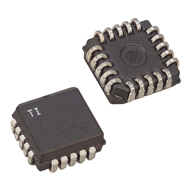
- Part No.:
- UC3707Q
- Manufacturer:
- Texas Instruments
- Category:
- Gate Drivers
- Package:
- 20-LCC (J-Lead)
- Datasheet:
-
 UC3707Q.pdf
- Description:
- IC GATE DRVR LOW-SIDE 20PLCC
- Quantity:
- Payment:

- Shipping:

Inventory:2,462
Please send an inquiry. Send us your inquiry, and we will respond immediately.
Product details
Overview
UC3707Q from Texas Instruments is a dual-channel high-speed power MOSFET driver IC designed for gate driving in switching power supplies and motor control circuits. It delivers ±1.5 A peak output current per channel, operates from 5 V to 40 V supply rails (VIN and VC independently), and features independent inverting/non-inverting inputs with analog shutdown capability and thermal protection. Its 20-pin PLCC package supports industrial temperature range (0°C to +70°C).
For engineers reviewing the UC3707Q datasheet, UC3707Q pinout, UC3707Q application, or UC3707Q equivalent, key selection considerations include its dual-channel totem-pole output architecture, 40 ns rise/fall time into 1000 pF, latchable analog shutdown function, and compatibility with discrete power MOSFETs in half-bridge and push-pull topologies.
Technical Context
The UC3707Q integrates two independent Schottky-process driver channels, each with separate input logic paths (inverting and non-inverting) and configurable shutdown via differential analog stop pins or digital shutdown pin. Its internal circuitry enables simultaneous or independent channel activation while preventing cross-conduction through low spike duration (25 ns) during VC transitions.
Shutdown behavior is programmable: analog stop inputs trigger latching or non-latching shutdown depending on the Latch Disable pin state, while the Shutdown pin provides hard override capability-forcing outputs low regardless of analog or latch status when driven high, and restoring normal operation when driven low.
Key Specifications
| Parameter | Value and Actual Design Meaning |
|---|---|
| Supply voltage range (VIN, VC) | 5 V to 40 V - Enables direct interface with wide-input DC-DC converters and battery systems without level-shifting. |
| Peak output current (per channel) | ±1.5 A - Sufficient to drive large gate capacitance MOSFETs (e.g., >2000 pF) with fast switching transitions. |
| Rise/fall time (10%–90%) | 25–50 ns into 1000 pF - Supports high-frequency PWM operation up to ~10 MHz in optimized layouts. |
| Analog shutdown threshold | 100–160 mV differential - Allows precise overcurrent sensing using low-value sense resistors without amplification. |
| Thermal shutdown trigger | 155°C junction temperature - Protects against sustained overload or inadequate heatsinking in enclosed environments. |
| Digital input thresholds | Low ≤0.8 V, High ≥2.2 V - Compatible with TTL and CMOS logic families across full supply range. |
| Operating temperature range | 0°C to +70°C - Qualified for commercial/industrial ambient conditions without derating. |
Pinout & Package
The UC3707Q is housed in a 20-pin plastic-leaded chip carrier (PLCC) package with gull-wing leads, moisture sensitivity level 2 (260°C peak reflow), and RoHS-compliant Cu/Sn finish.
| Pin/Terminal | Circuit Role | Design Meaning |
|---|---|---|
| 1, 2, 3, 4, 17, 18, 19, 20 | Ground (GND) | Eight dedicated ground terminals reduce common-impedance coupling and improve noise immunity between channels. |
| 5, 6 | Inverting Input (CH1, CH2) | Active-low logic inputs; drive respective output low when high, high when low - enables complementary drive configurations. |
| 7, 8 | Non-Inverting Input (CH1, CH2) | Active-high logic inputs; drive respective output high when high, low when low - supports standard PWM interface. |
| 9, 10 | Output (CH1, CH2) | Totem-pole outputs capable of sourcing/sinking ±1.5 A peak - directly drives N-channel MOSFET gates without external buffers. |
| 11 | Shutdown (SHDN) | Digital override input: high = forced shutdown (both outputs low); low = normal operation - bypasses analog latch logic. |
| 12 | Latch Disable (LD) | Controls analog shutdown behavior: low = latching mode (output stays low until reset); high = non-latching mode. |
| 13, 14 | Analog Stop (+, –) | Differential comparator inputs for analog shutdown - accepts small-signal voltage drop across current-sense resistor. |
| 15 | VIN | Logic supply input (5–40 V) - powers input stage and level-shifting circuitry; independent from VC rail. |
| 16 | VC | Driver supply input (5–40 V) - powers output stage; sets maximum gate drive voltage and output swing. |
Key Features
| Feature | Design Value |
|---|---|
| Dual independent totem-pole drivers | Enables asymmetric or synchronous half-bridge control without external isolation; eliminates need for discrete driver pairs. |
| Configurable analog shutdown with latch option | Supports both immediate fault recovery (non-latching) and lockout until manual reset (latching), reducing system-level supervision complexity. |
| Low cross-conduction current spike (25 ns) | Minimizes shoot-through risk during dead-time transitions in bridge circuits, improving efficiency and MOSFET reliability. |
| High-speed switching (40 ns into 1000 pF) | Reduces switching losses in high-frequency SMPS designs and enables faster transient response in motor gate drive applications. |
| Wide dual-supply operation (5–40 V) | Permits use with 12 V, 24 V, and 36 V industrial buses while maintaining full output drive strength across voltage range. |
Applications
| Switch-Mode Power Supply | Motor Drive Half-Bridge |
|---|---|
|
Use Scenario: Driving high-side and low-side N-channel MOSFETs in a synchronous buck converter operating at 200 kHz with 12 V input and 3.3 V output. IC Role / Device Role / Timing Role: Dual-channel gate driver providing complementary, non-overlapping gate signals with programmable dead time via external logic. Use Value: Delivers ±1.5 A peak current to charge/discharge 4.7 nF total gate capacitance within 50 ns, minimizing conduction loss and enabling >92% efficiency. |
Use Scenario: Controlling a 24 V brushed DC motor with bidirectional PWM using discrete N-channel MOSFETs in an H-bridge configuration. IC Role / Device Role / Timing Role: Independent channel driver enabling forward/reverse direction control and dynamic braking via coordinated CH1/CH2 activation. Use Value: Analog shutdown detects overcurrent via 10 mΩ sense resistor (100 mV threshold), triggering immediate latch-off to protect MOSFETs during stall conditions. |
| Induction Heating Inverter | UPS Inverter Stage |
|
Use Scenario: Driving resonant LLC half-bridge switches in a 3 kW induction heater operating at 150 kHz with 350 V DC bus. IC Role / Device Role / Timing Role: High-voltage gate driver interfacing microcontroller PWM with 600 V MOSFETs via isolated gate transformers. Use Value: 40 V VC rating allows direct connection to auxiliary 15 V bias supply; 40 ns switching ensures minimal overlap loss at high frequency. |
Use Scenario: Gate-driving IGBTs in a 1 kVA online UPS inverter delivering 230 V AC output from 48 V DC battery bank. IC Role / Device Role / Timing Role: Dual-channel driver supporting soft-start sequencing and overtemperature shutdown coordination with system controller. Use Value: Thermal shutdown at 155°C prevents IGBT failure during overload; shutdown pin enables centralized fault handling via MCU GPIO. |
Equivalent & Alternatives
The following parts are listed as comparable options for similar dual-channel gate driver applications.
| Alternative Part | Technical Difference | Application Difference | Selection Advice |
|---|---|---|---|
| UC2707Q | Identical pinout and electrical specs, but rated for –25°C to +85°C industrial temperature range instead of 0°C to +70°C. | Suitable for wider ambient environments including outdoor enclosures or unheated factory floors. | Select UC2707Q if extended low-temperature operation below 0°C is required; otherwise UC3707Q offers tighter cost/performance fit for commercial-grade systems. |
| UCC37322P | Single-channel, 4 A peak output, SOIC-8 package; lacks analog shutdown, latch disable, and dual-supply flexibility. | Requires two units for dual-channel use; no integrated fault management - external circuitry needed for overcurrent response. | Choose UCC37322P only for space-constrained single-MOSFET applications where high peak current (>1.5 A) is critical and fault handling is implemented externally. |
Compared with UC2707Q, UC3707Q trades extended temperature range for lower cost and tighter qualification scope; compared with UCC37322P, it integrates dual-channel control, analog fault detection, and latchable shutdown - reducing BOM count and improving system-level safety without sacrificing speed or drive strength.
Availability
UC3707Q is available at Aetrix Electronics and suitable for switch-mode power supplies, motor control inverters, induction heating systems, and uninterruptible power supplies requiring stable component supply and long-term industrial availability.
Supply support for UC3707Q includes scheduled delivery planning, volume procurement assistance, BOM continuity management, traceable sourcing, and lifecycle availability coordination for OEM customers, industrial embedded developers, connected-device designers, and electronics production programs.
Manufacturer
Texas Instruments is a global semiconductor company headquartered in Dallas, Texas, specializing in analog, embedded processing, and power management technologies with over 50 years of innovation in industrial and automotive electronics.
The UC3707Q belongs to TI's legacy power driver family designed specifically for robust, high-current gate driving in industrial switching applications where reliability, thermal resilience, and analog fault integration are critical.
FAQ
What is the maximum gate capacitance the UC3707Q can drive while maintaining 50 ns rise time?
The UC3707Q achieves 25–50 ns rise/fall times into 1000 pF load, as specified in typical switching characteristics. For heavier loads, rise time scales approximately linearly with capacitance; driving 4700 pF yields ~235 ns rise time under same conditions. To maintain sub-50 ns performance, keep total gate + Miller capacitance below 1000 pF or add external gate resistors to control ringing without compromising speed. The UC3707Q datasheet confirms this behavior across VIN = VC = 20 V and TA = 25°C.
Does the UC3707Q support bootstrap high-side drive configurations?
No, the UC3707Q does not integrate bootstrap diode or floating supply circuitry. It requires separate, isolated VC and VIN supplies for high-side operation. When used in half-bridge topologies, the high-side VC rail must be generated externally-e.g., via charge pump or isolated DC-DC converter-since the UC3707Q lacks internal level-shifting capability. This design choice ensures robustness in high-dV/dt environments but mandates careful PCB layout for gate loop inductance and supply decoupling. The UC3707Q truth table and connection diagrams confirm dual-supply dependency.
How does the analog shutdown function differ from the digital shutdown pin in UC3707Q?
Analog shutdown uses differential inputs (pins 13/14) to monitor a small-signal voltage (100–160 mV threshold) for overcurrent or overtemperature events, with behavior modulated by the Latch Disable pin. Digital shutdown (pin 11) overrides all analog logic: a high signal forces both outputs low unconditionally, while a low signal restores normal operation regardless of analog inputs or latch state. This separation allows layered protection-e.g., fast digital fault clearing during startup, plus precise analog trip during steady-state operation. The UC3707Q shutdown circuit description explicitly defines this hierarchy.
Can UC3707Q operate with VIN = 5 V and VC = 40 V simultaneously?
Yes, the UC3707Q supports independent supply rails: VIN (logic supply) may be set to 5 V while VC (driver supply) operates at 40 V. This configuration enables low-power microcontroller interfacing (e.g., 3.3 V or 5 V GPIO) while delivering full 40 V gate drive to high-voltage MOSFETs. Electrical characteristics tables confirm VIN and VC ratings are specified separately, and the block diagram shows isolated supply domains. However, ensure proper decoupling on both rails and verify that logic-level translation is handled externally if VIN < VC logic thresholds require adjustment.
Is the UC3707Q pin-compatible with UC2707Q or UC1707J?
No, UC3707Q is not pin-compatible with UC2707Q or UC1707J. While all three share functional similarity, UC3707Q and UC2707Q use 20-pin PLCC (FN) packaging, whereas UC1707J uses 16-pin CDIP (J). Even among PLCC variants, UC3707Q and UC2707Q share identical pinouts per TI's package drawings, but UC1707J's 16-pin layout differs fundamentally-e.g., fewer ground pins and merged functionality. Always consult TI's SLUS177B datasheet connection diagrams and package addendum before substitution. The UC3707Q datasheet explicitly lists FN as its sole PLCC variant.
UC3707Q Specifications
- Product attributes
- Attribute value
- Manufacturer:
- Texas Instruments
- Series:
- -
- Package/Case:
- 20-LCC (J-Lead)
- Packaging:
- Tube
- Product Status:
- Obsolete
- Programmable:
- Not Verified
- Driven Configuration:
- Low-Side
- Channel Type:
- Independent
- Number of Drivers:
- 2
- Gate Type:
- N-Channel MOSFET
- Voltage - Supply:
- 5V ~ 40V
- Logic Voltage - VIL, VIH:
- 0.8V, 2.2V
- Current - Peak Output (Source, Sink):
- 1.5A, 1.5A
- Input Type:
- Inverting, Non-Inverting
- High Side Voltage - Max (Bootstrap):
- -
- Rise / Fall Time (Typ):
- 40ns, 40ns
- Operating Temperature:
- 0°C ~ 70°C (TA)
- Grade:
- -
- Qualification:
- -
- Mounting Type:
- Surface Mount
- Supplier Device Package:
- 20-PLCC (9x9)
UC3707Q FAQ
1.How can I place an order for UC3707Q through Aetrix?
Please submit a Request for Quotation (RFQ) for UC3707Q on Aetrix. Our sales agent will provide a competitive quotation and guide you through the order confirmation once you accept the terms.
2.Are the price and stock information for UC3707Q reliable?
The price and inventory of UC3707Q are updated periodically and may fluctuate due to market conditions. Stock and pricing data are typically refreshed every 24 hours. Quotation validity for UC3707Q is usually 5 days.
3.What payment methods are accepted for UC3707Q?
We accept Wire Transfer, PayPal, Credit Card, Western Union, MoneyGram, and Escrow for UC3707Q transactions.
Note: Certain payment methods may incur a processing fee.
4.How is shipping managed for UC3707Q?
UC3707Q orders can be shipped via leading logistics carriers, including DHL, UPS, FedEx, TNT, or Registered Mail.
Once your UC3707Q order is processed, you will receive an email with the shipment details and tracking number.
Note: Tracking information may take up to 24 hours to appear. Express delivery typically takes 3–5 business days.
5.How can I obtain technical support or documentation for UC3707Q?
For technical support, including UC3707Q datasheets, pinout diagrams, or application guidance, please contact our engineering support team. They can provide detailed documentation and assistance for your UC3707Q requirements.
6.How does Aetrix verify that UC3707Q is sourced from the original manufacturer or authorized distributors?
All UC3707Q products on Aetrix are procured from qualified distributors and authorized channels. Our dedicated quality assurance team conducts strict verification, including traceability checks and, if necessary, third-party testing. This ensures that UC3707Q meets industry standards.
7.What is the process for return or replacement of UC3707Q?
All UC3707Q units undergo pre-shipment inspection (PSI). If there is an issue with UC3707Q, returns or replacements are accepted under the following conditions:
1.Quantity discrepancies, incorrect items, or visible external defects (such as breakage or corrosion), acknowledged by Aetrix.
2.The issue is reported within 90 days of delivery.
3.The UC3707Q part is unused and in its original packaging.
Return procedure for UC3707Q:
1.Submit a request within 90 days.
2.Obtain a Return Material Authorization (RMA) from Aetrix.
UC3707Q Tags

-
ZXGD3009E6TA
Diodes Incorporated
-
1EDN7512BXTSA1
Infineon Technologies

-
UCC27517DBVR
Texas Instruments

-
MCP1416T-E/OT
Microchip Technology
-
MCP1402T-E/OT
Microchip Technology
-
MCP1415T-E/OT
Microchip Technology
-
MCP1401T-E/OT
Microchip Technology
-
IX4428NTR
Littelfuse Inc.

-
IRS2005STRPBF
Infineon Technologies
-
IRS2008STRPBF
Infineon Technologies
-
IX4310TTR
Littelfuse Inc.

-
2EDN7524RXTMA1
Infineon Technologies
Tech Hub

A practical engineering guide to 3.3V and 5V logic compatibility, input thresholds, resistor dividers, translator ICs, MOSFET level shifting, I2C pull-ups, timing limits and power-sequencing risks.

The 74HC595 uses push-pull logic outputs, while the TPIC6B595 uses 50 V open-drain DMOS sinks for higher-power loads. This guide compares timing, current limits, 3.3 V interfacing, load wiring, thermal…

The 74HC595 converts serial data into eight stable parallel outputs. This guide covers pin functions, shift and storage timing, OE and MR behavior, drive-current limits, cascading, voltage compatibilit…

A technical comparison of level-sensitive latches and edge-triggered flip-flops, covering timing windows, setup and hold limits, master–slave operation, time borrowing, race-through, HDL inference and…

A D latch stores one bit while Enable controls when data can pass. This reference covers gate-level operation, truth tables, transparency, setup and hold timing, LE versus OE, common ICs and practical …

An SR latch stores one bit through cross-coupled feedback. This engineering reference covers NOR and NAND implementations, truth tables, forbidden-state recovery, gated operation, switch debouncing, fa…

Latch circuits retain one bit through feedback. This technical reference covers SR and D latches, truth tables, transparency, timing limits, latch-versus-flip-flop behavior, applications and common log…

An engineering guide to LED driver operation, constant-current and constant-voltage outputs, linear and switching topologies, dimming, IC selection, calculations, replacement compatibility, and fault c…

Operational amplifier guide covering op amp basics, feedback, ideal vs real op amps, common configurations, buffer circuits, offset, bias current, gain-bandwidth, slew rate, rail-to-rail limits and sel…

Jumper cables guide covering safe connection order, red and black clamp placement, final ground connection, cable gauge, length, clamp quality, copper vs CCA cables, jump starter comparison and battery…


